Ultra-Wide-Bandgap Power for Military Electronics
Insights | 08-07-2025 | By Gary Elinoff
Key Takeaways Ultra-Wide-Bandgap Power: Gallium-Oxide & Diamond Devices for Military Systems:
- Gallium Oxide and Diamond are Ultra Wide Bandgap materials
- The wide bandgaps, in excess of those characteristic of WBGs such as SiC and GaN, offer game-changing potential
- Gallium Oxide devices are now available in limited quantities
- The availability of practical Diamond semiconductors, offering even greater potential, is significantly further off
Introduction
Readers of these pages are likely already familiar with semiconductors based on silicon carbide (SiC) and gallium nitride (GaN). When compared to transistors based on silicon, these devices can handle greater voltages and operate at higher frequencies.
GaN and SiC can be described as wide-bandgap semiconductors. Simply put, these materials exhibit a "wide gap" between their conduction and valence bands. The energy that it takes to breach that barrier is -3.3 electron volts (eV) and -3.4 eV in SiC and GaN, respectively. This compares to 1.12 eV for silicon, the classic semiconductor material. It is this characteristic that endows SiC and GaN with their superior power and speed characteristics vis-à-vis silicon.
But new upcoming applications, such as hypersonic avionics and directed energy weaponry, will demand semiconductors that can outperform even SiC and GaN. This is where ultra-wide bandgap semiconductors (UWBG) will come into play. The two most promising materials are diamond and gallium oxide (Ga2O3), with bandgaps of -4.8 and –5.5, respectively.
In this blog, we'll examine the potential of semiconductors built of these novel materials, and the still significant barriers to commercialization. We'll now delve into characteristics of semiconductors fabricated with Gallium Oxide and with Diamond, and look into some of their use cases.
Gallium Oxide
As described by Nanotronics' Mathew Putnam in an article published in Forbes[1], semiconductors fabricated with Gallium Oxide have the potential to provide some very significant advantages as compared to present-day power semiconductors
- Reduced Energy Losses: Gallium Oxide's higher conductivity means that they will waste less energy, thus reducing parasitic heat, thus reducing cooling costs.
- Higher Voltage Operation: Semiconductors based on Ga2O3 will be able to operate at very high voltages, and higher voltages mean lower power losses.
- Higher Temperature Operation. Gallium Oxide transistors can operate at higher temperatures than other WPGs
- Higher Frequency operation. This is important because one of the main uses for WBGs or UWBGs is voltage level conversions. This is achieved largely through a transistor turning ON and OFF thousands, or even hundreds of thousands, of times per second, creating very high-frequency voltage pulses. These pulses, when provided as input to a transformer's primary coils, create AC on the secondary output, which can readily be converted back to DC, with the voltage level determined by the turns ratio between primary and secondary coils. The value proposition is that the higher the frequency, the smaller the size of the transformer.
Putnam goes on to describe some limitations of Gallium Oxide.
- Material Defects. Gallium oxide crystals often suffer from defects that affect device performance.
- Reliability. Designers are not yet confident of the long-term reliability of gallium oxide devices under high-voltage and high-temperature conditions.
- Thermal Management. While it seems contradictory, although gallium oxide can operate at high temperatures, its thermal conductivity is actually lower. Provisions have to be made to remove the heat from the device.
- Doping Limitations. P-type doping of gallium oxide has thus far proven to be difficult, limiting the types of devices that can be fabricated.
- Cost. Gallium Oxide devices are expensive to produce.
Semiconductors based on Gallium Oxide
These devices are only in the very first stages of commercialization. Eight inch wafers are standard in the semiconductor, and the successful fabrication of an eight inch Ga2O3 wafer will mark a significant milestone towards that end. China's Hangzhou Gallium Semiconductor claims to have done so. And, as reported by Japan's Novel Crystal Technology[2], the company hasn't hit the 8 inch mark yet, but it has produced 6 inch wafers.
A Note of Caution
It must be pointed out that in the semiconductor industry, reports of "wafer production" of any given size often only means the production of the same sized raw crystal. This intermediary still needs to be further processed into an actual wafer that can actually be used for device fabrication.
Equating raw crystals with wafers might seem to be a somewhat dubious claim, but the production of a crystal of the appropriate size is seen as a major milestone, and those in the know are aware of this seeming incongruity. Presently, actual Ga2O3 wafers that are ready for final fabrication are generally sized at two or four inches.
As it stands now, there is limited commercial production of Gallium Oxide semiconductors. These promising devices feature RDS(ON) values even lower than SiC or GaN, which foretell very low power losses. However, dealing with any heat generated will be problematic.
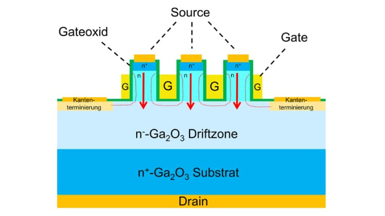
Gallium Oxide Semiconductor. Image source: Ferdinand Braun Institute
Institutions and companies involved in Gallium Oxide semiconductors include:
- Novel Crystal Technology
- Flosfia (Kyoto University)
- Fraunhofer
- Kyma Technologies
Diamond
Yes, diamond is a semiconductor. It has the most radical properties of any UWBG material currently being explored so far for power semiconductor fabrication.
Diamond as a Semiconductor (Key Properties):
| Property | Diamond | SiC | GaN | Ga₂O₃ |
|---|---|---|---|---|
| Bandgap (eV) | 5.5 | ~3.3 | ~3.4 | ~4.8–4.9 |
| Critical Field (MV/cm) | ~10 | ~3 | ~3.3 | ~8 |
| Thermal Conductivity (W/cm·K) | ~20–22 | ~4.9 | ~1.3 | ~0.2 |
| Electron Mobility (cm²/V·s) | ~2200 | ~950 | ~1500 | ~300 |
| Breakdown Voltage | Highest theoretical | Very high | Very high | Extremely high |
Chart provided through AI analysis
These properties make diamond perhaps the ultimate theoretical power semiconductor, ideal for ultra-high-power, high-temperature applications. Diamond-fabricated devices are extremely radiation-resistant and will eventually find uses in space vehicles and within nuclear reactors.
There are many hurdles to commercialization:
- Doping diamonds is very difficult, especially P-type doping, as is the case with gallium oxide.
- Diamond wafers are difficult and expensive to synthesize.
- Device fabrication steps, such as contact formation and etching, are proving to be troublesome.
- Semiconductors based on diamond are not expected to be in production for at least the rest of this decade.
But, even in present-day early-stage development, Diamond-based devices operating at temperatures in excess of 300℃ in high radiation environments have been demonstrated. Particularly notable is Diamond's very high thermal conductivity, which is far ahead of any other WBG or UWBG contender. It also features the highest bandgap at -5.5 eV.
Organizations Involved in Diamond-based Semiconductors Include:
- De Beers Group is a supplier of synthetic diamonds used in the development
- Fraunhofer
- National Institute for Materials Science (Japan)
- Kyoto University
- NASA Glenn Research Center
The Present and the Future for UWBG Devices
Diamond UWBGs promise the highest bandgap, highest breakdown voltage as well as remarkable thermal conductivity. However, production of actual devices is likely to be at least five years away. The first Gallium Oxide devices are just beginning to trickle out, but they are nowhere near large scale application.
As described by NASA[3], "Ga2O3 devices offer higher temperature operation, lower on-resistance, higher breakdown voltages, and higher power conversion efficiency than Silicon power devices. However, their performance in the space environment, including high-energy radiation and wide temperature fluctuations, is largely unknown."
Wrapping Up
Gallium Oxide and Diamond are both Ultra Wide Bandgap semiconductor materials. They have demonstrated characteristics that exceed Silicon Carbide and Gallium Nitride, the two most advanced wide bandgap semiconductors now widely available.
The two new semiconductor UWBG technologies feature higher operating voltages, radiation hardness and power handling capacities than current WBGs. They can both operate in high temperature environments, but Gallium Oxide does a relatively poor job of dissipating heat.
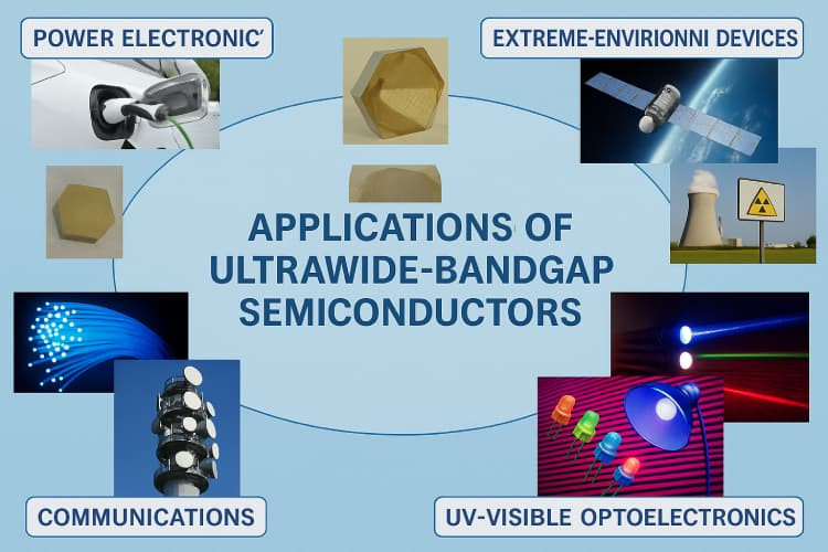
Both technologies will have huge applications in military and space technology, as well as in civilian applications. Gallium Oxide devices are starting to make limited appearances, but Diamond devices are still years away.
Challenges and Opportunities
Clearly, Diamond and Gallium Oxide-based semiconductors are a long way from being routinely available. While diamond-based devices are years away, Ga2O3 units are now just beginning to appear, but are held back in no small measure by the lack of stable eight-inch wafers. The former represent a major step forward from present day WBGs, while Diamond devices have the potential to be game changers.
What UWBG devices promise is radiation tolerance, high power and high speed, and will have a transformative effect on military technology
- Laser weapons, for example, will need to scale up on a massive scale if they are to be useful. Present day devices, in the hundred kilowatt range, are only effective at short ranges, and need to be focused on targets for far too long a time to be anything but interesting curiosities.
- Nuclear reactors will be safer and more efficient with semiconductors able to operate in the harshest radiation environments. Similar arguments can be made for vehicles operating the hostile environment of space.
- Servers are taking ever greater amounts of electricity to operate. The efficiency promised by UWBGs will serve to lessen the toll.
- Phased-Array Satellite Uplinks require multiple transmitters to operate in close proximity. Heat is now a limiting factor. The problems will only worsen as uplinks will need more power to track more objects at greater distances, moving ever faster in our hypersonic future.
And the list goes on.
SiC and GaN are making enormous contributions to military capabilities. UWBGs will push the envelope even further. The opportunities are monumental, and Gallium Oxide development seems to be moving ahead under its own steam; Diamond technology not so much. Considering the revolutionary potential of Diamond based semiconductors, it must be hoped that industry and the military not only continue funding this technology but increase the development efforts.
References
- Why Gallium Oxide Can Help Deliver A Sustainable AI Future. Forbes
- Novel Crystal Technology Achieves Breakthrough in Ga2O3 Crystal Growth, Paving Way for Larger, Higher-Quality Wafers. Novel Crystal Technology
- High-Voltage Gallium Oxide Devices for Space Power Electronics – 20027. NASA
Glossary of Terms
- RDS(ON). This key parameter is a measure of the source-to-drain resistance of a MOSFET when the device is in the ON state.
- UWBG (Ultra Wide Bandgap) Semiconductors. These devices offer bandgaps in excess of WBG (wide bandgap) semiconductors such as SiC and GaN.