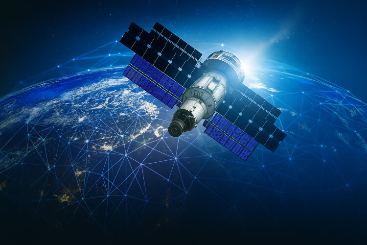
Space-Grade GaN: Powering Next-Gen Defence Satellites
Insights | 13-06-2025 | By Gary Elinoff
Key Takeaways about Space-Grade GaN: Enabling the Next Generation of Defence Satellite:
- Gallium Nitride (GaN) is a type of wide bandgap semiconductor, alongside of SiC
- The technology has inherently good resistance to radiation, which can be enhanced through augmented processing
- GaN transistors are highly efficient, a side benefit of which is that they give off little heat
- They can switch ON and OFF very quickly, making them adaptable power conversion applications
- They can operate at extremely high frequencies for satellite communication applications
Introduction
The Earth is protected from space-borne radiation by its magnetic field and by its atmosphere. The planet’s magnetic field forms a shield against charged particles from the sun and elsewhere. Some of the charged particles are trapped in a formation known as the Van Allen radiation belt, which itself provides another layer of defense. The atmosphere offers still more protection, shielding the planet’s surface from harmful cosmic and UV radiation.
Space vehicles travel far above the embrace of these protections, which begat a need for semiconductors resistant to radiation. For this reason, designers of space-based military communications satellites are turning to Gallium Nitride (GaN) semiconductors.
Compared to last-generation Silicon (Si) based semiconductors, space-grade GaN semiconductors offer superior resistance to many types and intensities of radiation. Additionally, they can operate at higher RF frequencies, and when used as “Switches”, they can turn ON and OFF far faster for more efficient power conversion. GaN devices of all types have a higher power density than other types of semiconductors, which means that for the same size and weight, they can handle far more power. Because saving space and weight are among the most critical requirements for any device launched by rockets into space, this advantage is of vital importance.
But before we get into specifics. Let’s take a short dive into the basics of GaN and Wide Bandgap Semiconductors.
What are Wide Bandgap Semiconductors?
GaN and Silicon Carbide (SiC) are both wide bandgap semiconductors (WBG), which we describe in detail in our previous blog, Wide Bandgap Semiconductors: The Key to Modern Military Technology. Basically speaking, “Wide bandgap semiconductors (WBG) are based on materials with a wide gap between their conduction and valence bands. This is the source of the ability to handle more power for devices of the same size as gallium arsenide or silicon semiconductors. And compared to old-school Silicon, WBGs can operate at higher frequencies.”
A key difference between GaN and SiC is that the former is faster, while the latter can handle more power. Additionally, the structure of GaN offers inherent resistance to radiation, even before the special processing offered by some manufacturers for GaN semiconductors destined for use in space vehicles.
More about GaN’s Resistance to Radiation
There are three primary radiation threats that semiconductors in space may be subject to:
- Single event Effects (SEE). When a semiconductor is subject to a one-time bombardment of high-energy particles.
- Displacement Damage (DD). Cumulative long-term radiation damage. Semiconductor material damage is affected by protons or neutrons displacing atoms in a lattice.
- Total Ionizing Dose (TID). Cumulative long-term radiation damage.
GaN’s wide bandgap (-3.4 eV, as compared to Silicon’s -1.1 eV) makes it harder for ionizing radiation to damage its atomic structure. As such, it offers excellent resistance to TID or SEE damage, and GaN also stands up well to DD.
Power Conversion
Within almost every type of electrical or electronic system, there is a need to convert voltages from one level to another. Most space vehicles, for instance, are powered by on-board solar power arrays generating DC power. That voltage will need to be converted to the voltage of the satellite’s main power bus. Then, the bus voltage needs to be converted into levels compatible with the vehicle’s many subsystems.
We describe how this is achieved in terrestrial systems in our earlier blog entitled SiC and GaN Power Semiconductors Extend EV Driving Range. As described, the WGB semiconductor switches on and off several thousand times per second, changing DC into very high speed pulsating DC, which, through the process described, can be converted into DC at any voltage level needed.
Transformers and other electromagnetic components are required to implement these conversions. The size and weight of the required transformers required will be inversely proportional to the frequencies involved. Thus, because the GaN “switches” operate at high speed, these components will be smaller and will take up less space.
The rules are similar for satellite systems. Additionally, when a GaN used in a space-based power system switches ON, there is very little internal resistance. This means that very little power is wasted, and with greater efficiency, less parasitic heat is generated, resulting in less need for bulky, heavy heat sinks to deal with it.
GaN used in Phased-Array Satellite Uplinks
Phased array technology is a central component in a wide range of military and civilian use cases. GaN plays a key role here, too. But just what is a phased array?
1- A Phased Array is an electronically steered device that can be used to project UHF and Microwave signals in any direction. Unlike a classical radar system, the physical antenna itself isn’t rotated. Instead, the antenna system itself consists of many individual static antenna transmitters collectively controlled by a computer. By altering the power and phase of each individual transmitter and by taking advantage of processes known as constructive and destructive interference, a high-frequency radio beam can be directed in any direction.
2- An enormous advantage of phased arrays is that more than one beam can be generated at the same time, all pointing in different directions. In a similar manner, incoming radio transmissions, perhaps from satellites, can be received on the same platform.
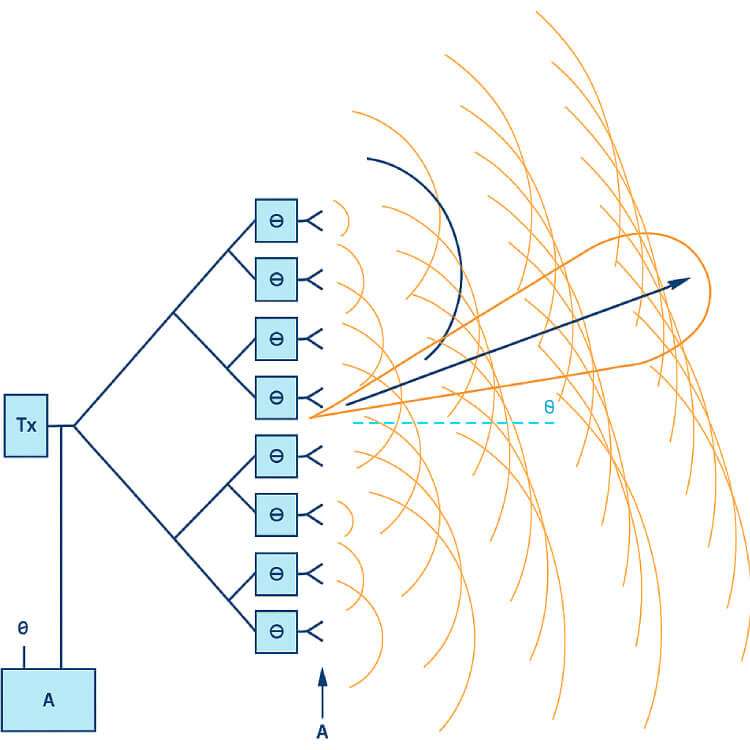
Figure 1. Basic Theory Diagram of Phased Array Elements.
3- With phased arrays, more than one satellite at a time can be tracked and controlled at the same time.
What Role Does GaN Play in Phased Arrays?
Phased array radars consist of many individual transmitters used to generate the RF beams described above; there can easily be 1000 separate transmitters or more. Each of these, separately energized by GaN-based Power Amplifiers (PA), are located immediately adjacent to the radiating element.
GaN is the ideal semiconductor type to be employed because:
- GaN’s high power density allows PAs to take up very little room, allowing for as many transmitting elements to be located as close to each other as needed.
- As described, the technology is very power efficient, and less heat-sinking is needed.
- GaN is resistant to radiation, making it ideal for satellite-based downlinks.
- GaN can handle the Ku-band (12–18 GHz), Ka-band (26–40 GHz), and Q/V-band (40–75 GHz) frequencies commonly employed in modern satellite communication.
- Gallium nitride devices are very linear, allowing them to handle even the most complex signal types, such as QAM and OFDM.
Space-Grade GaN
Space-grade GaN devices are much more expensive than standard GaN. Differences include:
- Space-grade GaN transistors are fabricated to provide even more protection against TID and SEE than standard GaN devices.
- They are subjected to screening for MIL-PRF-38535, MIL-PRF-19500, and ESA ESCC standards.
- To protect against moisture, they come in hermetically sealed ceramic or metal packages.
- They are designed to stand up to mechanical stress, and can operate over a -55°C to +125°C temperature range.
- They are extensively screened.
Manufacturers of Space Grade GaN include:
- Efficient Power Conversion (EPC)
- ST Microelectronics (ST)
- Qorvo
- Northrop Grumman
- GaN Systems
- Infineon
- Renesas
- Teledyne
- Texas Instruments
- Microchip Space
Wrapping Up
Satellites in space are subjected to radiation, and gallium nitride semiconductors are inherently radiation resistant, and through special selection and processing they can be designated to be space-grade. GaN semiconductors can switch fast in power conversion roles, and can handle RF in the Q/V-band in a communications role.
GaN devices, space-grade or not, can be tightly packed because they give off scant heat and are highly efficient. Their high power density suits them especially well suited for deployment on highly space-constrained military satellites.
These characteristics make them a natural choice for phased array communication links, on Earth as well as in space.
Challenges and Opportunities
Space-grade GaN devices are expensive to produce. Manufacturing yields can be quite low. Regulation is tough, with thorough testing and validation required. Radiation resistance will need to be even further improved if space-grade GaN technology is to be adequate for long duration flights in Geosynchronous orbit and beyond.
GaN in space doesn’t have a long-term track record yet, and designers are still leery about it. The stability of the device’s operating parameters under the totality of threats to be encountered in space has not as yet been sufficiently vetted.
Another headwind are standards, which have mostly been written for last generation silicon. GaN devices, space grade or not, often have to be examined individually to see if they’ll fit a particular set of circumstances.
The opportunities are literally as big as space. There is an ever-growing population of military and commercial satellites in orbit, and more ground stations to direct them. Ronald Reagan’s dream of “Star Wars” wasn’t possible when he first came up with the idea because the technology simply wasn’t there yet. Only this time around, it may just be possible thanks in part to advances in space-grade Gallium Nitride. Mars might be on hold for a decade or two, but human expansion into space, which is a bit closer to Earth, is pressing right ahead.
Glossary of Terms
- Wide Bandgap Semiconductor (WBG). Devices made of material that features a large energy gap between their valence and conduction bands. This characteristic allows them to operate at higher speed, temperature and power than silicon devices can.
- Gallium Nitride (GaN). A WBG, GaN, is often compared to Silicon Carbide (SiC). GaN can’t handle quite as much power, but it’s faster.