Gallium Nitride on Silicon Chips Improves Power Electronics
Insights | 24-07-2025 | By Robin Mitchell
Key Things to Know:
- MIT researchers have developed a scalable method for integrating GaN transistors onto silicon chips using low-temperature copper-to-copper bonding.
- The technique avoids costly materials like gold and supports compatibility with existing CMOS foundries, reducing production barriers.
- Discrete GaN dielets reduce material waste and support sustainable fabrication, offering benefits for AI workloads, 5G networks, and green data centres.
- The hybrid chips offer improved efficiency, thermal performance, and high-frequency capability, with potential in data centres, mobile infrastructure, and quantum computing applications.
As our devices become faster, smarter, and more power-hungry, the silent workhorse behind every innovation—power electronics—faces unprecedented demands. From lightning-fast charging to high-efficiency computing and electric vehicles, the pressure to deliver more power in less space with less heat is rapidly reshaping the electronics landscape.
To meet this challenge, researchers at MIT have unveiled a promising new approach that could redefine how we build next-generation electronics: integrating gallium nitride (GaN) transistors directly onto silicon chips. But what makes this development so critical, how does it work, and what could it mean for the future of power electronics?
The Ongoing Power Challenge
Power electronics have always been the underdog of any electronics system, whose tireless efforts in the background help to supply all critical components with energy. Whether you are lighting up an LED or driving a server farm that is able to perform at the highest speeds, the reliability and efficiency of power management fundamentally determines whether your circuit will operate.
However, as we continue to crave processing power and instant charging, the demands on power electronics that keep everything stable are also growing at the same rate (if not faster). For example, the need to quickly charge your phone is quickly becoming non-negotiable, high-power CPUs are breaking new thermal barriers, and electric vehicles are guzzling electrons like there is no tomorrow. But these are not incremental changes; they are seismic changes that strain existing traditional silicon-based semiconductors.
While silicon has been very good at providing reasonable power envelopes, we are now running marathon speeds on a vintage bicycle. Two transistor technologies that are slowly replacing silicon are gallium nitride (GaN) and silicon carbide (SiC). Both technologies offer reduced losses and higher efficiency, but neither is a silver bullet. GaN can be a bit prone to voltage spikes, and while SiC can be extremely tough, it still suffers from packaging and cost issues. Furthermore, these materials are not as forgiving as silicon and can often require engineers to completely rethink their topologies (which is not a trivial feat).
The power puzzle presented by SiC and GaN also introduces new inverter designs, new driver circuits, and isolation techniques. To make matters worse, trying to integrate these devices into a system can be challenging, especially when considering that some of these power transistors are discrete devices, making it difficult to pack everything together in applications where space is precious.
However, the future won’t wait, and the next leap in performance will see engineers get a little apprehensive about the promise of slimmer, faster, and more efficient electronics. In the field of power electronics, standing still is the same as falling behind.
MIT Researchers Develop Scalable Method to Integrate Gallium Nitride on Silicon Chips
Researchers from the Massachusetts Institute of Technology (MIT), in collaboration with industry partners, have demonstrated a new, cost-effective method for integrating gallium nitride GaN transistors onto typical silicon CMOS chips. Such technology could help to improve power electronics and high-speed communications, thereby boosting their performance and efficiency.
According to MIT, this hybrid fabrication method could also bring direct benefits to emerging domains such as real-time deep learning and high-bandwidth video transmission, where energy-efficient, high-frequency operation is crucial. The team’s process enables tighter integration of GaN transistors with silicon-based logic, potentially enhancing system-level performance in AI workloads and data-intensive edge computing environments.
Gallium nitride is the world’s second most common semiconductor, just behind silicon. The unique properties of this semiconductor, such as its high electron mobility and thermal stability, make it ideal for applications including lighting, radar systems, and power electronics. However, the cost and complexity of integrating GaN with conventional silicon-based electronics have hindered widespread adoption.
Reducing Material Waste with Discrete GaN Integration
By introducing discrete GaN dielets rather than full GaN wafers, the approach avoids unnecessary material usage, aligning with sustainable engineering practices. This strategy supports a lower carbon footprint in semiconductor fabrication, which is increasingly becoming a factor in technology procurement decisions, especially for infrastructure tied to green computing initiatives.
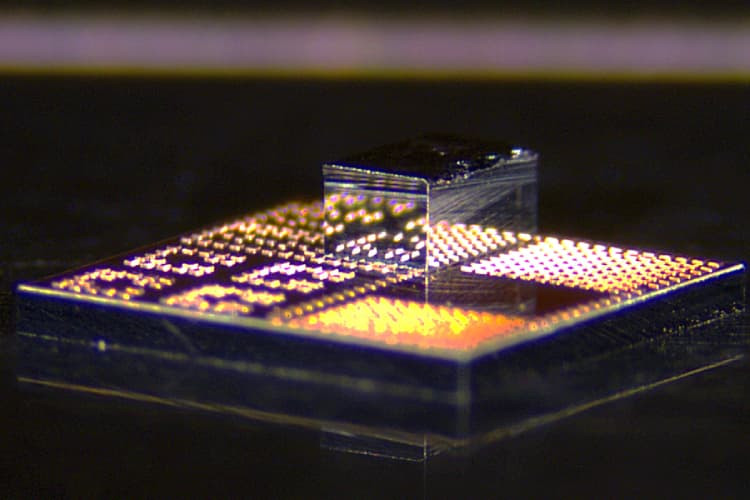
The new technique developed by the MIT researchers involves creating individual GaN transistor units, called dielets, which are then cut and bonded to silicon wafers using a low-temperature copper-to-copper bonding process. This method not only reduces material waste but also removes the need for expensive gold bonding and complex fabrication environments.
Low-Temperature Copper Bonding for Scalable Manufacturing
The bonding technique relies on copper-to-copper contact at sub-400°C temperatures, making it suitable for existing CMOS foundries without risking contamination or requiring exotic materials like gold. This compatibility means the integration process can scale industrially, allowing chipmakers to incorporate GaN’s performance advantages without overhauling legacy silicon manufacturing lines.
The combination of GaN’s speed and power capabilities with the mature digital processing capabilities of silicon will result in hybrid chips that are both more efficient and generate less heat. For example, the researchers have developed a power amplifier that provides higher signal strength and greater efficiency compared to similar designs using silicon alone.
Each GaN dielet is positioned using a high-precision robotic platform, aligning with nanometre-level accuracy before bonding. This controlled integration ensures consistent performance and opens up possibilities for RF system miniaturisation, particularly in mobile base stations and satellite communications, where space and thermal efficiency are at a premium.
Application Potential and Commercial Considerations
This scalable approach to integration could be useful in future data centers, high-frequency communication systems, and advanced power management systems. However, further research and development will be needed to determine whether it is commercially viable and stable over the long term.
The researchers presented these advancements at the IEEE Radio Frequency Integrated Circuits Symposium, highlighting the chips’ potential in wireless front-end modules. Independent experts, including Atom Watanabe from IBM, have noted that such heterogeneous integration techniques are instrumental in addressing the slow-down of Moore’s Law, offering a viable route to continue scaling system-level performance through architecture rather than transistor size alone.
How Could GaN on CMOS change electronics?
The use of GaN transistors directly on silicon CMOS chips is a significant step toward addressing many challenges faced by modern power electronics.
This hybrid solution combines the high electron mobility and power-handling capabilities of GaN with the mature manufacturing and processing infrastructure of silicon CMOS technology. This combination is expected to improve device efficiency, reduce heat generation, and enable more compact designs.
Practically, this could lead to power electronics that operate at higher frequencies and voltages while retaining a smaller footprint, which is critical for applications such as data centers and electric vehicles. Additionally, the improved efficiency and thermal management could extend device lifetimes and reduce overall energy consumption, aligning with the growing demand for sustainable technologies.
Furthermore, integrating GaN and silicon on the same chip can simplify system design by reducing reliance on discrete components and complex interconnections. This simplification could accelerate the development of new power amplifiers, converters, and communication modules that are not only more powerful but also more cost-effective and easier to manufacture.
However, this technology is still in its early stages, and several challenges remain, including ensuring long-term reliability, achieving consistency in large-scale production, and seamless integration with existing silicon-based systems. Continued research and development are needed to move GaN-on-CMOS solutions from laboratory prototypes to commercial-scale manufacturing.
Overall, the integration of GaN on silicon CMOS presents a promising future for power electronics. It offers a pathway to meet the rapidly increasing demands of modern electronics with devices that are faster, more efficient, and smaller than before. This advancement could enable future innovations across a wide range of technology sectors.
