Imec 6G Transistor Breakthrough on GaN-on-Si Platform
In The News | 19-06-2025 | By Matthew Walker

Key Takeaways:
- Imec has achieved record RF performance with a GaN-on-Si E-mode transistor, reaching 27.8dBm output power and 66% PAE at 13GHz.
- The device uses an 8-finger gate layout and InAlN barrier layer to enable high output power and efficient enhancement-mode operation on silicon.
- A separate contact module with record-low 0.024Ω·mm resistance could increase output power density by 70% when integrated.
- These developments bring GaN-on-Si technology closer to commercial readiness for energy-efficient, high-frequency 6G mobile applications.
Mobile networks are approaching the upper limits of sub-6GHz spectrum. To meet the data throughput and latency requirements of 6G, attention is turning to FR3—the frequency range spanning 7GHz to 24GHz.
However, operating at higher frequencies introduces new design challenges for RF front-end components in user equipment. Gallium arsenide (GaAs) heterojunction bipolar transistors (HBTs), a mainstay in today’s RF architectures, begin to lose efficiency and gain beyond 10 to 15GHz. This results in increased battery drain and reduced performance—two critical drawbacks for mobile applications.
The industry now faces a pressing need for RF technologies that can deliver high output power and efficiency at elevated frequencies, without compromising scalability or cost. Gallium nitride (GaN) has emerged as a strong candidate, offering high power density and breakdown voltage. But making it work for consumer mobile devices—particularly on silicon substrates—remains a significant hurdle.
The GaN Advantage—and Its Trade-offs
Gallium nitride (GaN) is widely recognised as a next-generation material for high-frequency RF applications. Its inherent advantages—high power density, wide bandgap, and excellent breakdown voltage—make it well-suited for demanding environments such as 6G.
In base station and infrastructure applications, GaN-on-silicon carbide (SiC) has already demonstrated strong RF performance at high frequencies. However, the high cost and limited wafer scalability of SiC limit its suitability for volume-driven mobile markets.
Silicon remains the preferred substrate for mass-market electronics due to its lower cost, mature fabrication ecosystem, and compatibility with large wafer sizes. Integrating GaN on silicon (GaN-on-Si) offers a promising path forward, but not without challenges.
The lattice and thermal mismatches between GaN and Si can degrade material quality and reliability. These issues are further compounded in enhancement-mode (E-mode) transistor designs—favoured in mobile applications for their normally-off behaviour and energy efficiency. Thinning the barrier and channel to enable E-mode operation often results in reduced on-current and increased leakage, compromising overall performance.
Imec’s Record-Breaking E-mode GaN-on-Si Device
Imec has announced a significant breakthrough in mobile RF transistor performance with a GaN-on-silicon enhancement-mode (E-mode) MOSHEMT. Operating at 13GHz with a 5V supply, the device delivers a record 27.8dBm output power and achieves 66% power-added efficiency (PAE)—setting a new benchmark for E-mode GaN-on-Si transistors.

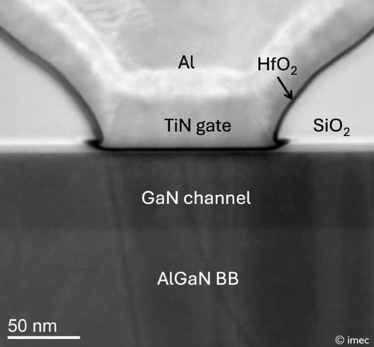
Cross-sectional TEM image of the gate structure in imec’s GaN-on-silicon transistor, highlighting the precisely etched gate region that facilitates enhancement-mode (E-mode) operation.
The device architecture uses an 8-finger gate layout to scale total gate width, enabling higher output power without relying on the combined performance of multiple transistors. This approach offers a streamlined path toward integrating high-performance RF transistors in space-constrained mobile front-end modules.
To achieve normally-off behaviour without compromising RF efficiency, Imec combined a gate recess technique with an indium aluminium nitride (InAlN) barrier layer. The gate recess shifts the threshold into E-mode, while the InAlN barrier compensates for the performance trade-offs typically associated with thinning the transistor channel.
Overcoming the Contact Resistance Barrier
Alongside its transistor development, Imec has demonstrated a record-low contact resistance of 0.024Ω·mm using a regrown n⁺(In)GaN contact layer. This marks a critical advancement in minimising power loss and enhancing current injection—both essential for high-efficiency RF operation at elevated frequencies.
Developed as a separate process module, the low-resistance contact is fully compatible with the E-mode GaN-on-Si MOSHEMT architecture. This modular approach enables performance scaling without the need for fundamental changes to the existing device structure.
According to device simulations, integrating this contact module into the E-mode transistor could yield a 70% increase in output power density. This would bring the technology within reach of key performance targets for 6G user equipment, where both power efficiency and form factor are critical.
The Road Ahead: Toward Real-World 6G Devices
Imec’s next step is the integration of its record-low contact resistance module into the E-mode GaN-on-Si MOSHEMT. This move is aimed at validating the simulated gains in output power and efficiency under real-world conditions—an essential milestone for eventual commercial adoption in mobile 6G systems.
As power amplifiers in user equipment must deliver high performance within tight thermal and energy constraints, combining output power with efficiency is non-negotiable. Achieving this balance on a silicon platform could give GaN-on-Si a decisive advantage in cost-sensitive, high-volume applications such as smartphones, tablets, and compact IoT devices.
“Reducing contact resistance is crucial for pushing output power while keeping efficiency high,” said Alireza Alian, Principal Member of Technical Staff at imec. “Our next step is to integrate this contact module into the E-mode transistor and validate the expected gains in power and efficiency, bringing the device closer to real-world 6G applications.”
A Step Closer to 6G-Era Mobile Hardware
Imec’s dual breakthroughs—a high-performance E-mode GaN-on-Si transistor and an ultra-low contact resistance module—represent a significant stride toward enabling GaN RF technology for mobile applications. Together, these developments address two of the most persistent challenges in deploying GaN at scale: efficiency degradation in enhancement-mode devices and contact losses that limit power delivery.
By combining performance, integration compatibility, and scalability on a silicon platform, Imec’s approach brings GaN-on-Si closer to viability for 6G mobile hardware. For handset manufacturers, RFIC designers, and wireless infrastructure developers, this work could open the door to smaller, more efficient, and more capable front-end architectures optimised for next-generation frequency bands.
Read More:
GaN vs Silicon: A Semiconductor Showdown on Efficiency
Examines the efficiency advantages of GaN over traditional silicon in power and RF applications, and where each technology fits in future designs.
What Will Win the Battle of the Bandgap: GaN or SiC?
Compares GaN and SiC in high-voltage and high-frequency domains, exploring their potential to dominate emerging power electronics markets.
The Evolution of GaN in Power Electronics
Tracks the development of GaN technology from early niche use cases to its growing presence in consumer and industrial power systems.
SiC and GaN Power Semiconductors Boost EV Driving Ranges & Consumer Electronics
Explores how wide-bandgap semiconductors are extending battery life and improving efficiency in electric vehicles and next-gen devices.

