Samsung's June 2023 Reveal: Enhanced 3nm & 4nm Chip Fabrication Process
In The News | 30-05-2023 | By Robin Mitchell
Times are exciting for Samsung as it gets ready to demonstrate its latest breakthroughs in 3nm and 4nm technologies in June. What challenges does shrinking transistors present, what can be expected from Samsung’s new nodes, and does this mean that Moore’s Law continues to persist?
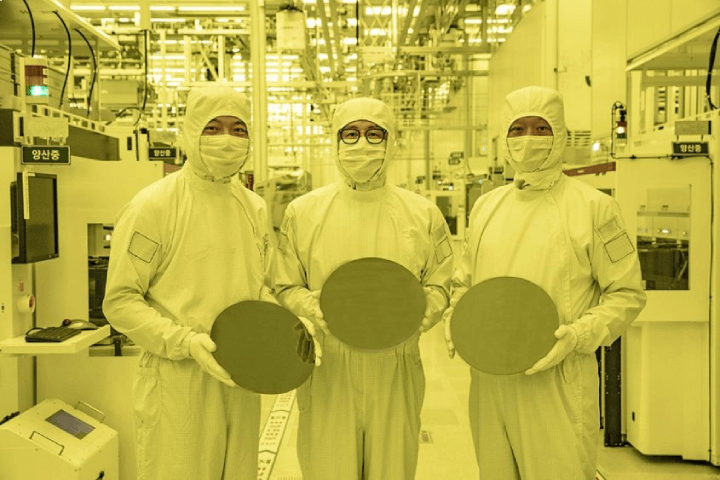
From left to right, Corporate Vice President Michael Jeong, Corporate Executive Vice President Ja-Hum Ku, and Corporate Vice President Sang Bom Kang of Samsung Foundry Business proudly display 3nm wafers on the production line at Samsung Electronics' Hwaseong Campus.
What challenges do shrinking transistors present?
As technology continues to advance at a rapid pace, the field of electronics has seen a consistent trend of shrinking transistor sizes. This trend, known as Moore’s Law, has driven the development of increasingly powerful and compact electronic devices. However, as transistors approach atomic scales, a new set of challenges emerges.
The first primary challenge that shrinking transistors encounter is the physical limitations of the universe that impede their performance. For example, the phenomenon known as quantum tunnelling allows electrons to tunnel through barriers, especially gates, leading to leakage currents as well as poor transistor operation. This effect reduces the reliability and efficiency of transistors, posing a major hurdle for further size reduction.
The second challenge that shrinking transistors experience is the problem of heat dissipation. As the size of a transistor decreases, the density of transistors on a chip increases, leading to higher power densities. This concentration of heat generates thermal hotspots, which can degrade transistor performance and even induce failures. Cooling these densely packed circuits becomes increasingly difficult, thus requiring innovative solutions such as advanced cooling techniques and materials.
The third challenge faced by semiconductor foundries is the manufacturing process itself. Traditional lithography techniques, which use light to pattern transistors on a silicon wafer, face limitations due to the diffraction of light, and at extremely small scales, the wavelength of light becomes comparable to the transistor dimensions, resulting in reduced accuracy and resolution. New techniques, such as extreme ultraviolet (EUV) lithography, have been developed to overcome this challenge, but these technologies are so incredibly advanced that only one company in the world, ASML, has the ability to produce such machinery.
The fourth challenge that engineers encounter is the physical limitations of semiconductor materials. For instance, traditional silicon-based transistors encounter increased resistance and leakage currents at smaller scales, leading to reduced performance. Exploring alternative materials, such as carbon nanotubes or graphene, holds promise but involves significant research and development to overcome their own limitations and integrate them into large-scale manufacturing processes. Thus, modern devices continue to be reliant on silicon as a semiconductor material.
A more unusual concern for shrinking semiconductors is their overall reliability. At smaller scales, transistors become more susceptible to various forms of degradation, such as electromigration, ageing, and even quantum effects. These factors can lead to a decrease in the lifespan and overall performance of the transistors.
Finally, reducing the size of transistors also significantly increases the complexity of designs and the tools used to make them. Integrated circuits with billions (or even trillions) of transistors require advanced tools and methodologies, and just like the machines used to fabricate semiconductors, not many companies are able to provide such systems. For example, verification, testing, and debugging of these complex designs become increasingly challenging, requiring massive amounts of computational resources.
Overall, engineers are faced with monumental challenges when developing semiconductors, and only with massive amounts of funding, effort, and research can engineers accomplish the goal of reducing transistors. These challenges were discussed in depth at the 2023 Symposium on VLSI Technology and Circuits Workshops, where leading experts in the field presented their latest research and findings.
Samsung to announce 3nm and 4nm nodes
As TSMC continues to push its 3nm node process, other semiconductor foundries are desperate to get to 3nm so as not to fall behind. Recently, Samsung announced that it would be unveiling its new 3nm and 4nm processes in June, something that has the engineering community buzzing with excitement.
Dr. Siyoung Choi, President and Head of Foundry Business at Samsung Electronics, stated, 'Samsung has grown rapidly as we continue to demonstrate leadership in applying next-generation technologies to manufacturing, such as foundry industry’s first High-K Metal Gate, FinFET, as well as EUV. We seek to continue this leadership with the world’s first 3nm process with the MBCFET™'1.
The first process being launched, called SF4X, is Samsung’s fourth-generation 4nm process that provides a multitude of improvements over its first-generation 4nm technologies. For example, the new transistors using the SF4X process are expected to offer engineers a 23% increase in power efficiency compared to the previous SF4 process.
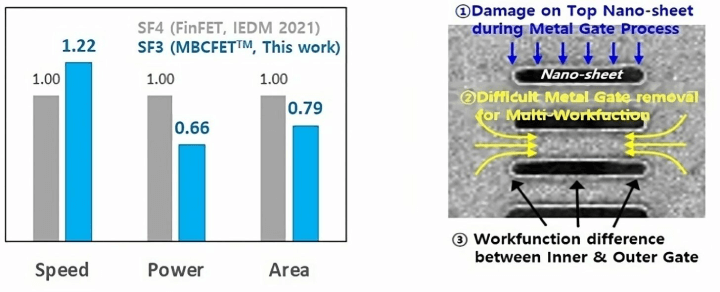
The second process, called SF3, will utilise Samsung’s 3nm GAP technology as well as Gate All Around transistors for improved gate performance (as transistors at this scale struggle to use traditional planar gates). However, instead of calling it Gate All Around, Samsung specifically refers to this construction style as Multi-Bridge-Channel Field-Effect Transistors.
Additionally, the SF3 process will be 22% faster than SF4 when operating at the same power and will provide an increase in power efficiency of 34% when using the same number of transistors and operating frequency. Finally, the SF3 process will reduce the total area used by 21%, allowing for increased logic density.
Samsung's 3nm process technology employs a Gate-All-Around (GAA) transistor architecture, a first in the industry. This architecture, known as Multi-Bridge-Channel FET (MBCFET™), overcomes the performance limitations of FinFET by reducing the supply voltage level and increasing drive current capability, thereby improving power efficiency1."
According to the 2023 Symposium on VLSI Technology and Circuits Workshops, Samsung's new 3nm and 4nm processes are expected to feature advanced FinFET technology, which offers superior performance and power efficiency compared to traditional planar transistors. This technology allows for a more precise control of the electric current, resulting in faster and more energy-efficient chips.
Samsung officially announced the start of its initial production of the 3nm process node applying Gate-All-Around (GAA) transistor architecture in June 20221.
Does this mean that Moore’s Law continues to persist?
While Gordon Moore may have passed away recently, his legacy continues, and his concept of Moore’s Law, which sees the number of transistors doubling on any given die every 18 months, is still holding true (albeit slowing down as transistors reach the nanometer scale). Eventually, however, transistors will reach a point where they cannot be shrunk reliably, and engineers will have to look at new solutions to increase the power and performance capabilities of semiconductors.
It is highly likely that in the next decade, chiplets will be used to not only increase the transistor count of a single package but also provide flexibility to engineers. Engineers needing chiplets can arrange to have dies sent from different semiconductor manufacturers to a single fabrication house, and specialised substrates with die interconnects will allow chiplet packages to be built in a similar fashion to custom PCBs.
It is also possible that 3D semiconductors will become crucial in future designs. By increasing the number of transistor layers, it is possible to massively increase the transistor count without having to shrink the size of features. In fact, it is possible for 3D devices to increase the size of transistors to help ease the manufacturing process. However, 3D devices come with numerous challenges, so whether they become a mainstream technology is yet to be seen (memory technologies such as NAND flash use vertically stacked transistors, but this is not the same as logic elements that need to be connected together in arbitrary ways).
Overall, Samsung continues to demonstrate its technological capabilities with its improved process nodes, and fierce competition between it, Intel, and TSMC will certainly yield exciting results in the future.
References:
