IBM announces Vertical FET – Why going up matters
| 21-12-2021 | By Robin Mitchell
Recently, researchers from IBM and Samsung have jointly developed a new semiconductor technology called VTFET that claims will help to increase transistor counts. What is VTFET, why is going up instead of out extremely important, and how will VTFET change the industry?
What is VTFET?
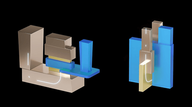
Vertical Field-Effect Transistors, or VTFET for short, is a new semiconductor technology that has been recently announced by IBM and Samsung that was developed as a joint venture. Standard transistors are planar and rely on features made in a silicon wafer’s X and Y plane.
A VTFET, however, uses vertical standing structures to create transistors meaning that they use the Z plane for their transistor action. Simply defined, a VTFET stands for Vertical Transistor Field-Effect Transistor, and it puts a transistor on its side to make the current flow vertically through the transistor’s source, drain, and gate.
3D stacking technologies already exist, with one recent example being Intel’s vertically stacked CMOS gates. However, the difference between VTFET and these is that the gate and channel are vertically stacked, meaning that there is no lateral flow of electrical current. This reduces the total footprint of a single transistor and hence allows more transistors to fit on a 2D plane.
Why is going up instead of out so extremely important?
Since their development, semiconductors have relied on the ability to shrink transistors to increase the total number of transistors on a design. This increased transistor count results in more complex circuitry and incidentally also reduces the power consumption, which can aid in creating low-energy devices.
How transistors have been traditionally constructed demonstrates why going vertical is so important. A traditional transistor is a planar device and relies on features created in the X and Y planes (for reference, the Z plane moves away from a flat silicon disc while X and Y move along the disc).
Generally speaking, the performance of a transistor is very much dependent on its physical dimensions in the X and Y plane because these are the directions in which current flows, so trying to make them as small as possible introduces challenges such as quantum tunnelling. However, the X and Y-plane transistor dimensions must be reduced to get the most transistors on a wafer. Thus, there is a trade-off between transistor size and transistor characteristics.
The X and Y planes are essential to the physical dimensions of a die (and thus the number of transistors), but the height of a chip (the Z plane) has never been an issue for engineers in any design because silicon dies are so thin. For this reason, going up instead of out could be critical for future designs.
By placing transistors vertically, there is almost no change in the die height (remember that transistors are nanometres in size), but the amount of space used in the X and Y plane is significantly reduced. City construction is a good analogy for why going vertical is so essential. Cities are often limited in lateral space but have infinite space going upwards. By going up instead of out, less land is needed, and thus more buildings can be built.
How will VTFET change the future of designs?
The first change that will be noticed is that transistor density will suddenly increase, allowing for more complex devices. But IBM has also announced that their new VTFET technology could be used to create energy-efficient devices such as smartphones that could last on battery power for a week, not for a day.
VTFET will not only impact data processing technologies, but it will also impact memory technologies and could potentially give rise to SRAM replacing DRAM. DRAM is used as a cheap memory technology with reasonable access times, but SRAM is significantly faster while not requiring refresh cycles. Furthermore, SRAM does not require write-back, whereas DRAM is destructively read.
While VTFET is an impressive technology that will help power the most advanced devices, it will unlikely be used in everyday electronics such as basic microcontrollers and analog devices simply because it is unnecessary. A commonly overlooked fact is that most electronics on the planet are built using decades-old technology (between 250nm and 100nm), as it is still a viable technology.
Overall, VTFET is a promising step towards increased transistor counts for the next generation of devices. It may not be deployed for the next few years, but its development could lead to highly advanced computing systems that focus more on specialised hardware units to perform specific tasks instead of generic computing devices that can do any task.
