How Do Modern Technologies Help Prototyping
| 12-08-2020 | By Robin Mitchell
The advances in technologies have resulted in components almost too small to be usable by most, and yet prototyping has never been easier. What modern technologies aid prototyping and how cheap has prototyping become?
Shrinking Technology - Smaller, More Powerful Devices
Since the introduction of electricity, it is truly amazing to see how far electronics has come. The first transistors, which would be mounted in large three-pin packages, can now be fabricated in the nanometres, with billions fitting on a single chip. Axial resistors have been replaced with SMD chip resistors measuring just millimetres across, and entire computer systems are now available on credit card-sized single-board computers.
Creating a new design requires several stages of prototypes which can demonstrate critical errors, flaws, and realities of the end product. For example, a conceptual design for a computer might have a PCB that is only 10cm x 10cm, but the resulting prototype demonstrates poor heat dissipation properties. In the past, building prototypes would require mostly hands-on work with components being soldered on, and product casings being machined. However, all of the work was relatively easy thanks to the use of through-hole technology, large components, and generally large designs. A classic example that demonstrates the ability to add last-minute changes to a design can be found in the ZX Spectrum; a transistor needed to be added across the Z80 processor.
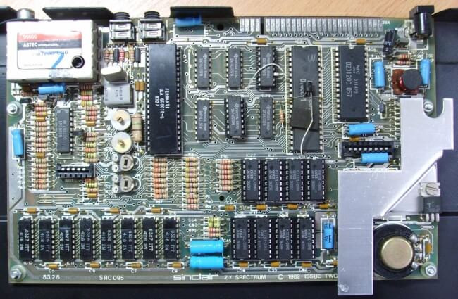
Credit: tomdalby.com
However, changes in technology have seen components move away from their larger, through-hole varieties in favour of tiny SMD (surface mount device) parts that are near invisible to the naked eye. This causes problems for several reasons; the most crucial being that modern circuits are almost impossible to build by hand. Large SMD parts do exist (such as SOIC, QFP, and 1206), but generally speaking, end products try to use the smallest possible devices as these are often the cheapest to use. Not only do they use less material, but they use less PCB (printed circuit board) space, meaning that the PCB can be reduced in size, and this leads to further reductions in cost.
You would be forgiven to think that prototyping in this new age of electronics is near-impossible, but this could not be further from the truth. As technology improves, so does the ability to use that technology, and a whole range of methods that used to be inaccessible to the broader public are now becoming commonplace in even the most basic of projects!
Read More
PCBs - Printed Circuit Boards
PCB technology has come a long way, but not for the reasons you would think. In the past, many prototypes would be designed using stripboard, matrix board, and even breadboards. Such methods are perfectly adequate for through-hole parts, but cannot be used when dealing with SMDs. Chip converters do exist, which allow a user to solder an integrated circuit (IC) to a PCB which connects the pads on the IC to pin headers for use in breadboards, but these are not appropriate for passive components such as resistors, capacitors, and inductors.
One solution in the past to this was to use a PCB, but these were incredibly expensive, and something that only businesses could afford. Homemade PCBs (utilising various chemicals such as Ferric Chloride), could allow makers to create intricate designs using SMD parts, but these had their flaw. For instance, through-hole plating was not achievable due to the complex chemical processes needed, and thus designs utilising more than one layer would be difficult to manufacture.
However, the start of 2010 saw a new era of prototyping, and the cost of professionally made PCBs began to drop rapidly. Instead of hundreds of dollars, makers can now get multiple prototype PCBs for a few dollars, enabling them to efficiently work with SMD parts, 4-layer PCBs, and through-hole plating. The reason for this reduction in price? Continuing advancements in automation and production technology have allowed PCB manufacturers to group multiple customer designs, use parallel machines to perform the same tasks, and utilise effective Automatic Optical Inspection (AOI), to rapidly-produce quick prototype PCBs.
Read More
Prototyping 3D Printers
In many instances, designing and building the circuit is only half the task; many projects require product enclosures. Designs of the past would require intensive manual labour to develop mechanical drawings and build the prototype enclosure. The cost of the enclosure would depend on the material it was made from, but this price would dramatically increase as the complexity of the design increases. One method around this was to utilise pre-made project enclosures, which would provide designers with a standardised container with screw mountings, knock-outs, and access ports. However, such enclosures provide next to no customizability and would be only useful to products whose housing was irrelevant.
Move forward to today, and the scene changes completely. The first significant step that reduced the time needed to produce prototypes was the introduction of CAD; suddenly, designers could interact with their mechanical designs, use 3D visuals to check if a PCB would fit, where the connectors would be located, and how it would fit together. The use of CAD also significantly helps when linked to newer methods for production that utilise Computer Numeric Design (or CNC); instead of human operators, a design can be milled, drilled, cut, and sanded by a single machine.
However, the real innovation in prototyping is the introduction of the 3D printer. While 3D printing technology has been around for decades, essential patents have recently expired, and the result is a wave of 3D printing machines that any home operator can use. Instead of needing a specialist company to manufacture a casing, a single designer can use CAD to create a 3D model of the casing, and a 3D printer to print the casing in many different materials including plastic, wood, and metal.
Read More
Pick and Place
The introduction of SMD components also brought with it a new manufacturing technique; Pick and Place. These automated machines have components preloaded into reels, which are automatically imaged, picked up by a suction head, and then positioned onto the PCB. A camera performs an AOI on the PCB once done to ensure that all components have been placed correctly, and the board is then sent into a reflow oven to melt the solder paste to solder all the parts in one cycle. Such technology has been out of reach for individual makers due to the high setup costs, but some have built their Pick and Place machines (although these are far and few between).
However, companies such as JLCPCB have begun to offer pick and place prototyping services at incredibly low costs. One factor that helps to reduce the cost of such prototypes is the encouragement for makers to use standardised parts. For example, multiple projects designed by different designers will often require the same basic components; 0603 resistors, SMD capacitors, and a microcontroller, and by identifying the most commonly used components, the Pick and Place setup can be mostly left alone (i.e. no need for constant reel changes). This dramatically speeds up production time, and the ability to ship PCBs straight from the production facility to the manufacturing facility further reduces this cost.
Read More
Modules and Shields
The introduction of new ICs such as sensors can be exciting for makers, but only if they can get them into a prototype in the first place. Small SMD parts often require the use of a PCB, and developing the hardware support for an IC itself can be problematic. While some devices do come with example circuits, it is no guarantee that a particular design will work. Even if the hardware works, the cost for prototyping an individual IC can be somewhat excessive.
The benefits of cheap PCBs and low-cost Pick and Place machines has seen many modules and shield be produced for the very purpose of prototyping. These boards contain all the hardware needed to operate a specific IC, usually include pin headers and sockets, and are cheaply available. Such boards are easily connected to breadboard circuitry, but the use of standardised layouts such as the Arduino Shield allows for prototyping boards to be stacked on-top of microcontroller development boards.
How Modern Technologies Help Prototyping Methods - Final Thoughts
Modern technology brings plenty of advantages, but also comes with its challenges. The reduction in component size has made traditional prototyping more difficult, but if makers take advantage of low-cost PCB services, 3D printing, and the wide range of modules available, then any project can be tackled with ease.
