New Theory for Semiconductor Nanocrystals Revealed
Semiconductors | 16-07-2020 | By Robin Mitchell
Researchers from ETH have revealed their development of a theory that explains how nanocrystal semiconductors work. Why is this work necessary, and how will it help engineers of the future work with nanocrystals?
Traditional Semiconductor Theory
While semiconductors have been known to exist for a very long time, the discovery that they could be used in electronics was only discovered in the early 20th century. Since the creation of the first transistor, electronics has grown exponentially with modern life entirely reliant on semiconductors working in a particular way. To put into perspective the importance of semiconductors, if they were to be removed from the planet, then the result would be humanity going back to the 19th century with steam engines, the telegraph, and other mechanical systems. Technologies such as modern medicine, free information, instant communication, and computational systems would be non-existent. But how do semiconductors work, and how are engineers able to change their behaviour?
Semiconductors are materials whose resistance lies in-between conductors and insulators. The most commonly used material for modern semiconductors is silicon and is almost always used in its crystalline form. A semiconductor on its exhibits very little interesting properties being naturally intrinsic (i.e. no net charge), and as such cannot be used for anything practical. However, if the crystalline structure is doped with elements that have electron shells either nearly full or nearly empty, then the resulting interaction is that the crystal exhibits either a net positive or negative charge. Again, on their own, these materials are not particularly interesting, but when combined produce some fantastic results. Insulating barriers form between the boundaries which will only conduct electricity in one way (i.e. a diode), and electric charge can be used to control the flow of power (i.e. MOSFETs). The mechanisms that cause these effects are well known, and as such engineers can make silicon do pretty much anything they want whether it be to control the flow of current, emit light, or even tunnel electrons. However, a new type of semiconductor structure, called nanocrystals, do not behave in the same way, but a team of researchers may have cracked their secrets!
Nanocrystal Semiconductors
To start, a nanocrystal is a miniature crystal of a substance, and a nanocrystal semiconductor is a semiconductor material consisting of many nanocrystals side by side. In standard semiconductors, they can be modelled as particles moving through a uniform medium where impurities in the medium (i.e. dopants), affect how the medium works. In nanocrystal semiconductors, however, adding dopants does not always add charge carriers to the material, and this is the mechanism that allows for the changing of the material properties. This means that a nanocrystal structure can be thought of as a random medium whereby charge carriers can get stuck, hit bumps, and cause deformations. The ability for charge carriers to cause deformations in the nanocrystals, called polarons, changes the way the material fundamentally behaves, meaning that the entire charge carriers path through the material needs to be considered. This includes the interaction between each charge carrier with each atom in each nanocrystal.
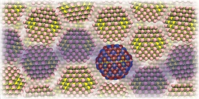
Tightly packed crystals in a nanocrystal semiconductor: the model developed by ETH researchers describe every single atom.
Credit: ETH Zurich / Nature Communications
The team of researchers, lead by Vanessa Wood, utilised the Swiss Supercomputing Center SCS in Lugano to model nanocrystal semiconductors to see what factors affect these materials the most. After running the complex code, which looks as how electrons get trapped and why they cant continue their journey through the material, the team were able to determine factors that affect electron mobility. According to the simulations, the main determining factor for electrical conduction are tiny deformations in the nanocrystals, and the tiniest deformation has a significant effect on the electrostatic energy.
To see if their research holds in the real world, the team of researchers created thin films of nanocrystals. It then measured the electric responses when different voltage and temperatures were applied. When free electrons were created on one side of the material (using laser pulses), the resulting electrical properties matched that of the simulations. It is hoped that the results from their research and experiments will help with further understanding of nanocrystal semiconductors, and how to exploit their characteristics to create more efficient electronic systems based on quantum dots.
“After eight years of intense work, we have now created a model that can finally quantitatively explain not just our experiments, but also those of many other research groups over the past years. Such a model will enable researchers and engineers in the future to calculate the properties of a nanocrystal semiconductor even before it is produced. This should make it possible to optimise such materials for particular applications. So far, this had to be done by trial and error.” - Vanessa Wood
