IBM & ASMPT: Hybrid Bonding Breakthrough for Chiplets
In The News | 14-06-2023 | By Robin Mitchell
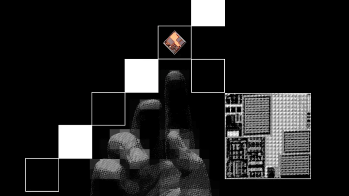
Chiplets present engineers with new opportunities in the field of semiconductors, but current bonding techniques introduce numerous challenges. Now, a joint venture between IBM and ASMPT has yielded a new hybrid bonding for packaging chips that allows dies to be directly bonded at an atomic scale, allowing for reduced contact sizes.
What challenges do chiplets face, what did the joint venture develop, and how could this help accelerate future chiplet designs?
What challenges do chiplets face?
As semiconductor manufacturers struggle to shrink the size of individual transistors, researchers are constantly looking for new methods for increasing the performance of modern devices. While one option is to make generic processors more powerful (with faster computational speeds and greater memory sizes), another option is to instead identify specific tasks that are resource intensive and create dedicated hardware accelerators. This use of hardware accelerators is already in widespread use, such as GPUs that process graphics routines, AI accelerators that are optimised for neural nets, and cryptographic accelerators that allow for encryption on-the-fly with no performance impact.
However, for all the benefits that accelerators provide, placing accelerators external to a chip has a massive impact on data bandwidth, but trying to integrate accelerators into a single monolithic semiconductor reduces the total area usable for other hardware, such as processor cores and memory. To solve this challenge, engineers are turning to chiplets, small individual semiconductor dies that have a specific purpose, and connecting these chiplets together to create an encapsulated module.
Not only does this allow engineers to make the most of silicon space on any one die, but it also allows for customisation, where chiplets can be swapped out for different devices, thereby allowing for full customisation of SoCs. But for all the advantages that chiplets bring, there is one major drawback that engineers are struggling to deal with; die interconnections.
In a recent blog post by IBM Research, they delve into the concept of chiplets and how they can help overcome these challenges. Chiplets are essentially smaller, functional blocks of a complex-function chip, which can include separate computational processors, graphics units, AI accelerators, and I/O functions. By breaking up the system-on-a-chip model, chiplets can lead to more energy-efficient systems, shorten system development cycle time, and build purpose-built computers for less than it would cost today.
One solution is to flip chiplets onto a substrate similar to a PCB and have the dies soldered to the substrate. However, due to limitations in current soldering technologies, pads on chips must be greater than tens of microns in size, and this restricts interconnect densities. At the same time, solder can be difficult to control, leading to poor-quality connections whose bandwidth is restricted.
IBM's second-generation nanosheet technology has paved a path to the 2 nm node, produced on a 300 mm wafer. This technology allows for the fitting of 50 billion transistors in a space roughly the size of a fingernail. The nanosheet transistor for the 2 nm chip node is a validation of several smaller milestones that proved this could be done and of the hard work and dedication of IBM’s interdisciplinary team of experts in materials, lithography, integration, devices, characterisation, and modelling working on the project.
Another option is to mount dies onto a substrate and use gold wires between dies. While this is commonly used with die bonding, it is an expensive process that may not be suitable for the low-volume production of customised chiplet designs. There are also practical limitations that can make bonding wires to dies complicated (as ending a bond wire can leave a tail which can move around and potentially cause shorting).
IBM and ASMPT develop a new chiplet bonding technique
Recognising the challenges faced with chiplet bonding, researchers from IBM and ASMPT have jointly developed a new solution that could help accelerate the deployment of chiplets. This new hybrid bonding for packaging chips allows dies to be directly bonded at an atomic scale.
IBM and ASMPT have made a significant breakthrough in chiplet bonding technology. They have developed a hybrid bonding technique that drastically reduces the size of the bonding needed between two chiplets. This is achieved by taking advantage of copper and oxide layers on an atomic scale, with the bond itself being only a few atoms thick. This development could potentially revolutionise the way chiplets are packaged and accelerate the deployment of chiplet technology.
To help bond chiplets, the research venture has developed a hybrid technique that takes advantage of copper and oxide layers on an atomic scale (with the bond itself being only a few atoms thick). However, in order for the bonding to work, it is essential that all moisture and debris is removed between the two surfaces, as even a few molecules of water are enough to impact electrical continuity between two contacts. This also applies to potential air bubbles that can form between two surfaces, as small pockets can easily hold gas molecules via electrostatic forces.
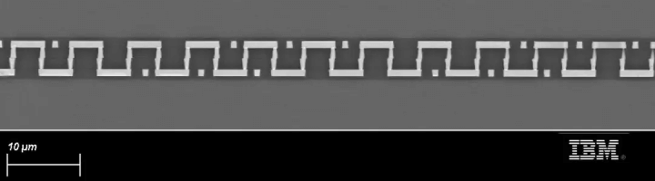
An image showcasing the minute bonding between two layers achieved through the team's method.
The hybrid bonding technique developed by IBM and ASMPT is a game-changer for the semiconductor industry. By reducing the size of the bonding needed between two chiplets to just a few atoms, this technique allows for a significant increase in the density of connections between two different dies. This, in turn, can lead to a substantial increase in data bandwidth, opening up new possibilities for the design and performance of semiconductor products.
The methods developed, according to the researchers, are extremely similar to existing die bonding methods used between different chiplets, however, at a much smaller scale. Additionally, the joint venture was able to achieve the bonding with pre-existing machinery provided by ASMPT, meaning that the new technique could potentially be deployed in the next few years.
How could such die-bonding techniques transform future technology?
By far, the biggest advantage offered by the newly developed bonding technique is that it significantly increases the density of connections between two different dies, thereby increasing data bandwidth. However, increasing the density of connections also allows for engineers to split up complex designs across multiple dies, and this not only helps to improve wafer yields but significantly increases the size of designs. This, in turn, increases the transistor count of large-scale semiconductor products, resulting in exponentially more powerful systems with increased processor and memory capabilities.
Additionally, the new bonding technique could also help accelerate semiconductor customisation for engineers. While still in its infancy, if the chiplet industry is anything like the PCB industry, it won’t be long before engineers are able to design their own SoCs in a near-identical fashion to customised PCBs with assembly services. Such a service would allow engineers to create a SoC that is catered to their application, integrating accelerators for key tasks while utilising low-energy options to reduce power consumption.
Overall, what IBM and ASMPT have developed is exciting for the chiplet industry. While more research needs to be done to ensure that the bonding technique is reliable and repeatable, this new hybrid bonding for packaging chips could potentially revolutionise the way semiconductors are designed and manufactured.
The development of this new hybrid bonding technique is a testament to the innovative work being done by researchers at IBM and ASMPT. It is a significant milestone in the field of chiplet technology and holds great promise for the future. As this technology continues to evolve, we can expect to see even more exciting developments in the way semiconductors are designed and manufactured.
IBM's research into chiplets is already showing promising results. They are exploring various designs for chiplet I/O based on the direction of the two main contenders for industry chiplet standards, the Universal Chiplet Interconnect Express (UCIe) Consortium, and the Bunch of Wires specification from the Open Compute Project. IBM researchers are involved with both initiatives, working on signal mapping strategies in the context of potential future chiplet packaging solutions. This proactive approach ensures that IBM will be ready to build chiplets as soon as standards are agreed upon.
References:
-
IBM Research Blog. (2023). "Hybrid Bonding for Chip Packaging and Chiplets." Retrieved from https://research.ibm.com/blog/hybrid-bonding-chip-packaging-chiplets
-
IBM Research Blog. (2023). "What are Computer Chiplets?" Retrieved from https://research.ibm.com/blog/what-are-computer-chiplets
-
IBM Research Blog. (2023). "2 nm Chip." Retrieved from https://research.ibm.com/blog/2-nm-chip
-
IBM Research Publications. (2023). "Voids-free Die-level Cu-Cu Hybrid Bonding." Retrieved from https://research.ibm.com/publications/voids-free-die-level-cuild-hybrid-bonding
