Intel Investing $3.5B in Advanced Packaging
| 20-05-2021 | By Robin Mitchell
Recently, Intel announced that it is going to be investing $3.5 billion into one of its fabrication facilities to utilise its proprietary packing technology Foveros 3D. So what are chiplets, what is Intel’s Foveros 3D technology, and why is Intel investing in the new packaging?
What are chiplets?
Reducing the size of transistors to fit more onto dies has been the main driving force for technological improvements since the first chips were designed. However, continuing this trend is becoming an increasing challenge as features approach the atomic scale. Therefore, designers are turning to new methods for creating devices with more processing capabilities.
One method that is being explored and implemented by some semiconductor foundries is the chiplet. Instead of squeezing more transistors onto a single die, a chip could be constructed with multiple chips connected together. While the resulting device will be physically larger, the small size of chips can make the size increase unnoticeable as far as the PCB that uses the chip is concerned.
Combining multiple chiplets comes with its own challenges, and there are many different ways to achieve this. One method involves stacking chips in a 3D sandwich with each chip having a specific function (such as processing, logic, and memory). Another method involves placing chiplets onto a carrier board (which can be thought of as a small PCB), where interconnects are used to connect the various chips together.
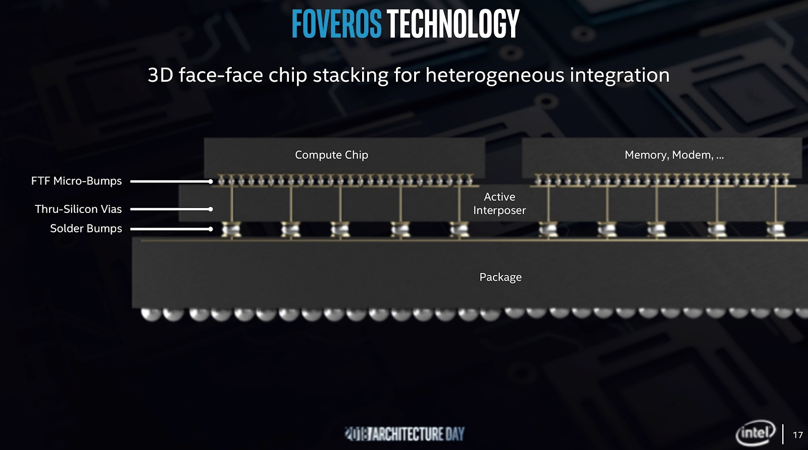
What is Intel’s Foveros 3D technology?
Intel, a world leader in semiconductor fabrication, have patented their own chiplet technology called Foveros. The Foveros 3D technology breaks up a design into multiple layers which are stacked on top of each other. The top-most layer is the compute logic layer which includes computing modules, FPGAs, memory, and RF controllers. The next layer is the basic logic die which holds logical components that are used to interconnect different compute chips together. For example, this layer would integrate bus decoders, dedicated communication channels, and buses. Finally, the third layer is the package substrate that connects the base logic die to the outside world using solder balls (i.e. BGA).
What makes the Foveros technology unique is the ability to connect dies face to face.OOlderhnology was reliant on connecting dies using wires and trace,s but these introduce long delays and degraded performance. Instead, Foveros connects dies together using FTF Micro-Bumps (i.e. miniature ball connectors), allowing two dies to be mounted directly onto each other. This technology also increases the number of connectors possible between dies, and therefore can dramatically increase bandwidth and segregation of systems.
Credit: Wikichip
Intel to Invest $3.5 Billion in Foveros Technology
Recently, Intel announced that it will be investing $3.5billion into its Rio Rancho foundry to enable the manufacture of Foveros 3D packaging. Not only is the funding being used to allow new packaging technologies, it will also be increasing the number of workers on the site by 35%. Intel intends to start the upgrade work by the end of 2021 and be releasing products using Foveros 3D stacking by late 2022.
This is not the only investment that Intel is committing to; Intel is also putting in more than $20 billion to revamp its foundries and create new ones. Intel’s recently slumped in the semiconductor market as a result of poor management which resulted in other foundries such as TSMC gaining a major lead. While many investors pressured Intel to go fabless, it decided to double down and go full ahead with its fabrication business. This move by Intel shows that it is serious about manufacturing semiconductors, and while 5nm and 7nm present challenges, the benefits of Foveros may outweigh those gained by using a smaller node.
Read More
