The Evolution of GaN in Consumer Electronics: Key Insights
Insights | 20-05-2024 | By Gary Elinoff
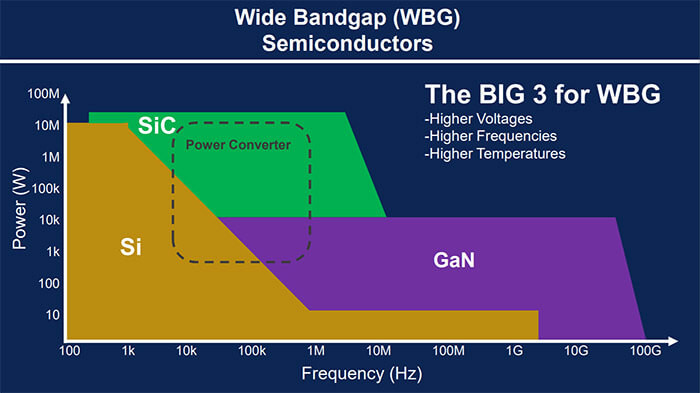
GaN compared to SiC and classical silicon. Modified Image source: AVNET
Key Takeaways about The Evolution of GaN in Consumer Electronics:
- Gallium Nitride (GaN) and Silicon Carbide (SiC) are technologies that are replacing Silicon-based power devices.
- GaN can "switch" faster but can't handle as much power as SiC can.
- SiC's great power capacity isn't needed for mobile devices, so faster, more efficient GaN is the usual choice for designers of low and mid-power devices.
Introduction
The Achilles Heel of today's electronic industry is the battery. Whether the small batteries for mobile devices, the big batteries for EVs or the gigantic batteries for utility-scale power, there is no area of science and engineering where progress is so slow despite massive a worldwide effort. Designers of consumer devices can just include a larger, heavier battery - but hey, wait, the watchword for consumer devices is smaller and lighter, so a bigger battery simply won't fly.
So, what's the solution? Design consumer devices to operate more efficiently. As we shall see, the key to that effort comes in the form of Wide-Bandgap semiconductor devices (WBG), and for consumer devices, the WBG of choice is Gallium Nitride (GaN).
According to a detailed guide by Belkin, "Gallium nitride, or GaN, is a material that's starting to be used for semiconductors in chargers. It produces less heat, which means components can be closer together, making a charger smaller while maintaining all the power capabilities and safety standards."[2] This technological advancement is crucial in the quest for more efficient consumer devices.
What's so Special about Wide Bandgap Devices?
GaN, along with Silicon Carbide (SiC), is a member of a new class of devices known as Wide Bandgap Semiconductors (WBG). These devices differ from classical silicon semiconductors in that they can handle more power at higher voltages and operate at higher frequencies.
Also, when used in power supplies, semiconductors are configured to "switch" from "OFF" to completely "ON" and to offer as little electrical resistance to the flow of current as possible in the ON state. WBG devices offer far less resistance than last-generation silicon does.
GaN Systems highlights that "In 800V battery-based traction inverters, the adoption of GaN-based three-level topology (3LT) is a growing trend." This advancement underscores the exceptional efficiency of GaN technology, which not only minimises switching losses but also reduces the high-frequency losses in filters and motors, resulting in more efficient power delivery systems.[3]
So, why are frequency and ON State Resistance so Important?
Frequency
The higher the operating frequency of a semiconductor device, the faster it can "switch" from ON to OFF – conducting electricity or not conducting electricity. This switching converts the electrical input to the semiconductor to pulses of DC output. The frequency of this "Pulsating DC" is directly proportional to the switching frequency, and the faster the switching, the more closely spaced the pulses of DC that the semiconductor delivers in a given period. Converting those pulses into the clean, stable DC voltage that consumer power supplies and power converters need requires a filter that often consists of relatively bulky inductors and capacitors.
Belkin's analysis reveals that "GaN is different. It's a crystal-like material that's capable of conducting far higher voltages. Electrical current can pass through components made from GaN faster than silicon, which leads to even faster processing."[2] This property is essential for high-frequency applications, making GaN a preferred choice for modern power electronics.
As it turns out, faster-frequency electrical pulses require smaller filters, which take up a disproportionate amount of space in mobile devices. Thus, higher-frequency switching and the smaller filters required make for smaller, lighter consumer devices.
Lower ON Resistances
When wide bandgap devices turn ON, there is less internal resistance across the device than there would be with silicon units. Current flowing across resistance generates power, but it's wasted power in this case because it never leaves the semiconductor. Rather, it is trapped within as heat, so this power is not only wasted but also further vexes engineers who need to provide heat amelioration, which will again make for a larger, heavier device.
The specifications of GaN and SiC are constantly improving, as manufacturers around the world are putting huge efforts into power semiconductor R&D. However, the main thing that doesn't change is that SiC can handle more power than GaN, but it can't operate at frequencies quite as high.
This discussion centers around consumer devices that will not require the huge amounts of power that SiC can conduct. As such, this examination will center around GaN, which, as noted, can switch even faster than SiC can.
GaN-Based Fast Charging Devices
The not-so-hidden secret to fast charging is a higher charging current. Because of the greater efficiency of GaN transistors, smaller, lighter chargers based on this technology can deliver that current to power-hungry smartphones, tablets, and laptops.
Because of fast charging, even small devices require more power than the 5 watts a typical silicon charger of yesteryear could provide. Charging protocols were developed for safety and to avoid pushing in too much or too little power during any device's charging cycle phase. Charging protocols are quite sophisticated, as there is much two-way communication between the charger and the device under charge. The expanding universe of devices to be charged supports a range of charging protocols, such as Power Delivery (PD) and Quick Charge (QC), which complicates the interface issue.
Because modern consumers would not tolerate carrying separate chargers for each different mobile device, most current GaN-based fast charging devices support multiple protocols. However, users would be well advised to be sure the charger to be purchased supports the specific protocol for the target mobile device(s). This step is, indeed, a necessity because, as described in an article published in CNN[1], "It's been about four years since the likes of Apple, Samsung, and Google stopped including a free wall charger with new smartphones."
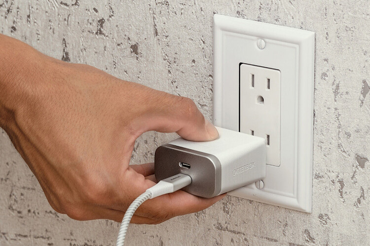
A 30-watt charger that is about the same size as the last generation's 5-watt device. Image source: CNN
Often relying on USB-C port(s) for the fastest charging, USB-A ports are often provided by even modern chargers to accommodate older devices.
An important point to keep in mind about GaN fast charging devices is that even if you bought a 300 charger to partner with a powerful laptop, because of the protocols, it is safe to use that device to charge a smartphone with a much smaller power budget.
GaN-Based Compact Power Adapters
As pointed out by Belkin[2], "The main thing about GaN when it comes to chargers is that it produces less heat. Less heat means components can be closer together, so a charger can be smaller than ever before—while maintaining all the power capabilities and safety standards."
Moreover, as CNN's review of GaN chargers highlights, "It's been about four years since the likes of Apple, Samsung, and Google stopped including a free wall charger with new smartphones."[1] This shift emphasizes the growing importance of high-efficiency, compact chargers that can support multiple devices and protocols.
We mentioned the built-in monitoring systems that are a key part of any modern charger. Many newer mobile devices, too, support those protocols. In the same manner as a water pumping system that won't allow a flood, the charger–mobile device dyad won't allow overcharging.
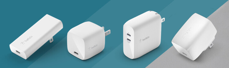
GaN wall chargers. Image source: Belkin
So, in essence, most compact power chargers can perform fast charging if the device to be charged is equipped with a protocol that allows it.
High-Efficiency Power Solutions
Because GaN can switch faster than SiC, it is more electrically efficient. So, if a given use case doesn't require more power than GaN can supply, it will generally be preferred over SiC. Indeed, GaN can even work in devices as demanding as EVs.
As pointed out by Infineon[3], GaN is even being used in 800V battery traction inverters, which are the main devices supplying juice that powers EVs. There is considerable evidence that GaN may be the preferred technology in this power range. In the same article[3], comparing a GaN inverter to a SiC-based inverter illustrated that "the 30kW inverter application demonstrated a 25% reduction in power loss and a 33% increase in power density with GaN compared to SiC. Several Tier1 and OEM automotive companies have realized similar results with traction designs up to 250kW."
Challenges and Opportunities
GaN and SiC devices do present design problems for engineers. Their gates are harder to drive than classical silicon devices, and the issues involved usually call for specialist power engineers. This has slowed down adaptation. Manufacturers have gotten around this issue by offering GaNs with gate drivers specifically designed for the individual SiC device. To make it even easier, the SiC and the driver are packaged together, which offers the additional benefit of saving board space and weight.
GaN Systems highlights the transformative impact of GaN in the EV sector: "In a collaboration with Toyota and Nagoya University, GaN increased power density and improved efficiency by 20% over silicon, extending the car’s driving range."[3] This exemplifies the potential of GaN technology to revolutionise power efficiency across various applications.
As it stands at the present time, cost is an issue for SiC devices. GaN offers lower thermal conductivity, which would be much more of an issue than it is, but for the excellent power efficiency that these devices offer.
One of the top priorities of the electronic industry is to reduce power consumption. As such, many OEMs are seeking to replace silicon power devices with GaN, even in existing designs.
Wrapping Up
GaN and SiC are both wide bandgap materials. They offer lower resistance from the semiconductor's source to its drain when the device is in the "ON" state than silicon-based devices do. They can both switch faster than silicon, but GaN is faster than SiC. On the flip side, SiC can handle more power.
Because both WBGs switch faster than silicon devices can, power modules based on these types of semiconductors require smaller output filters, resulting in smaller, lighter devices. Their lower RDS(ON)s means that they are more energy efficient, a sine qua non for today's electronic industry. The greater efficiency means less parasitic heat to deal with, again allowing for still smaller, lighter OEM final products.
References:
- These GaN chargers will juice up your phone, tablet or laptop super fast: https://www.cnn.com/cnn-underscored/electronics/best-gan-chargers
- What's GaN, and why do you need it?: https://www.belkin.com/products/product-resources/gan-chargers/
- GaN Advantages Growing in 400V and 800V EV Traction Design: https://gansystems.com/newsroom/gan-400v-800v-ev-traction/
Glossary of Key Terms:
- GaN. Gallium Nitride
- RDS(ON). The resistance from source to drain of a semiconductor device. One of the main advantages of wide bandgap semiconductor devices are exceptionally low RDS(ON)s
- SiC. Silicon Carbide
- WBG. Wide Bandgap Semiconductors