Ga2O3 Production Advances with UK Thin-Film Innovation
Insights | 06-05-2025 | By Robin Mitchell
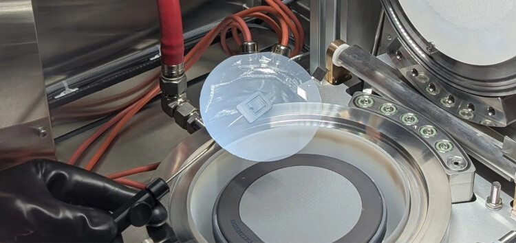
The AIXTRON close-coupled showerhead within the Oxide and Chalcogenide Metalorganic Chemical Vapor Deposition (MOCVD) reactor is depicted as the 4-inch gallium oxide thin film on sapphire is being removed.
While silicon has powered generations of electronic innovation, from the earliest microprocessors to today's smartphones, the limitations of this once-groundbreaking material are becoming increasingly evident. As the demand for faster, more efficient, and more durable components intensifies—particularly in areas such as electric vehicles, renewable energy, and high-frequency communications—the search for next-generation semiconductor materials has become a global priority.
Key Takeaways:
- Silicon has dominated semiconductor manufacturing for decades but struggles with high-speed, high-power applications.
- Alternative materials like graphene, SiC, and GaN offer faster operation and better thermal performance—but at higher costs and production complexity.
- UK researchers at Swansea University have developed the country’s first 4-inch thin-film gallium oxide (Ga₂O₃) capability.
- This breakthrough strengthens the UK's position in advanced power electronics and supports its growing semiconductor ecosystem.
What makes silicon insufficient for tomorrow’s electronics, which materials are emerging as front-runners, and how could a breakthrough by UK researchers in gallium oxide (Ga₂O₃) manufacturing reshape the future of power electronics?
The Race for New Semiconductor Materials
For decades, silicon has been the backbone of the electronics industry, providing engineers with a material that is not only cheap and easy to produce but also highly adaptable. Its ability to be easily integrated into a wide range of applications has seen silicon dominate the industry, from the first computers to the latest smartphones. But for all the benefits provided by silicon, there are a number of challenges that it faces, and as such, the race for new semiconductor materials is on.
One of the biggest challenges faced by silicon is that it is not capable of producing extremely high-speed electronics. While it is possible to create high-speed silicon devices, they are often extremely expensive and power-hungry, making them impractical for everyday use. In contrast, other materials, such as graphene, have the potential to create devices that operate at terahertz frequencies, which would be a major step forward for the electronics industry. Furthermore, graphene is also much more flexible than silicon, making it ideal for use in flexible electronics.
Another challenge faced by silicon is its poor thermal and voltage breakdown capabilities. While it is possible for silicon devices to be designed to operate at high voltages and temperatures, they are often bulky and power-hungry. This can be a major issue for applications that require high-power devices, such as electric vehicles and renewable energy systems. In contrast, other semiconductor materials, such as silicon carbide (SiC) and gallium nitride (GaN), have been shown to have much better thermal and voltage breakdown capabilities than silicon. As such, they are often used in high-power applications, and their use could help to improve the efficiency of power delivery in such applications.
SiC and GaN are often seen as the future of semiconductors, and as such, they have been the focus of many researchers and engineers. However, even these materials have their own challenges and are not able to replace silicon in all applications. For example, SiC and GaN devices are much more expensive than silicon devices, making them less practical for everyday use. Furthermore, SiC and GaN devices can be difficult to produce, which can make them more challenging to manufacture. As such, SiC and GaN devices are often used in niche applications, such as high-power transistors, but are not able to replace the ubiquitous silicon devices found in everyday electronics.
UK Researchers Develop New Process for Ga2O3 Production
Swansea University has made a crucial breakthrough in the field of semiconductor research, establishing the UK's first 4-inch thin-film gallium oxide (Ga2O3) capability. This development is a major step forward in the production of next-generation semiconductors that can efficiently support high voltages, power, and frequencies necessary for applications in electric vehicles and renewable energy sources.
According to Swansea University, the thin-film Ga2O3 capability was achieved using a newly commissioned AIXTRON close-coupled showerhead deposition system. This tool enables precision growth of high-quality crystalline films on 4-inch wafers—a first for the UK semiconductor landscape.
Breakthrough in Thin-Film Ga₂O₃ Technology
The system, located in the university's Oxide and Chalcogenide MOCVD Laboratory, demonstrates the UK's capacity to contribute to advanced power electronics, including devices essential for electric vehicles and 5G infrastructure.
The achievement was made possible with the commissioning of a state-of-the-art Aixtron close-coupled showerhead deposition system, which can precisely produce high-quality crystalline thin-film gallium oxides on 4-inch substrates, also known as wafers. The newly developed thin-film gallium-oxide wafers have been tested and found to be very uniform, with extremely high quality.
This high uniformity in gallium oxide film quality is essential for ensuring the performance reliability of semiconductor components under high-stress electrical environments. Researchers highlighted its relevance in deep-UV photodetectors and transparent conductive oxide layers, enabling multi-functional device engineering.
This cutting-edge capability is housed in the newly established Oxide and Chalcogen Metal-Organic Chemical Vapor Deposition (MOCVD) laboratory at the Centre for Integrated Semiconductor Materials (CISM). The laboratory is set to become a national centre for thin-film gallium research and development, focusing on applications such as power electronics, high-frequency photodetectors, and transparent conductive oxides.
As highlighted by Dr Dan Lamb, the Oxide and Chalcogenide MOCVD Centre opens new collaborative pathways for research in materials science. The lab aims to serve as a national hub, supporting both academic and industrial R&D in next-generation semiconductors.
Building a National Research Hub for Advanced Semiconductors
The development of thin-film gallium semiconductors is a crucial step toward creating more efficient, compact, cost-effective electronic devices. This achievement also demonstrates the growing capabilities of the South Wales semiconductor cluster, which is home to globally leading semiconductor manufacturing companies, including Vishay, KLA-Tencor, Microchip, and IQE. The establishment of the MOCVD laboratory is a notable milestone in the region's efforts to expand its semiconductor manufacturing capabilities.
This aligns with the strategic goals of the South Wales semiconductor cluster, which includes global industry players like Vishay and IQE. The expansion of Ga2O3 capabilities enhances the UK's position in the global race for wide-bandgap semiconductor technologies, a field increasingly critical to electrification and net-zero targets.
The achievement is also timely, given the recent announcement of a £250 million investment by Vishay in its Newport plant, supported by the UK government's automotive transformation fund. This investment aims to expand the production of advanced wide-bandgap power semiconductor components, further solidifying the region's position in the semiconductor industry.
Industry Impact and Strategic Investments
Sam Evans, Director at Vishay Newport, noted that the MOCVD expansion directly supports regional ambitions for wide-bandgap material innovation. The £250 million investment is expected to fast-track domestic manufacturing in silicon carbide and gallium oxide devices for power-dense applications.
According to Professor John Heffernan of the National Epitaxial Facility, which supports semiconductor-related research in UK universities, Swansea University's MOCVD capability is accessible to researchers through direct collaborations. Researchers can also gain direct access to feasibility studies through a partnership between Swansea University and the UK National Epitaxial Facilities' pump-priming scheme. The scheme ensures that academic and industrial partnerships can leverage Swansea University's expertise in epitaxial film growth to accelerate their own research and technology development.
The integration with the National Epitaxy Facility allows universities and commercial partners to access Swansea’s MOCVD system under the Pump Priming scheme. This ensures smaller research groups can test ideas without prohibitive equipment investment, promoting innovation across the UK semiconductor sector.
Dr. Dan Lamb, research lead for the Oxide and Chalcogen MOCVD Centre at the University of Swansea, expressed his excitement about the possibilities offered by the new facility. The advanced equipment will enable researchers to push the boundaries of existing work while creating new opportunities for collaboration between research groups across the UK.
Sam Evans, Director of QA and External Affairs at Vishay Newport, also welcomed the development, highlighting the importance of the South Wales semiconductor sector. The establishment of the new facility represents a major advancement for wide-bandgap materials innovation, supporting efforts to grow regional manufacturing capabilities in advanced power electronics.
The £2.7 million grant from the Engineering and Physical Sciences Research Council (EPSRC) that funded this system also reflects broader government support for UK semiconductor resilience. Such initiatives underscore the strategic importance of materials innovation for long-term industrial competitiveness.
The UK's Future In Semiconductors – Could It Exist?
The development of Ga2O3 thin films is undeniably crucial for creating more efficient, compact electronic devices, and the exhibiting the 400mm thin-film Ga capability by the researchers at Swansea University is a notable step forward in this direction. But the demonstration of UK capabilities in the field of semiconductors also introduces a possible new direction; enabling the UK to become a semiconductor leader.
The ability to produce advanced semiconductor materials will give the UK the potential to compete with other countries, such as Japan and South Korea, in the production of high-end electronic devices. The development of Ga2O3 materials will also help to create new job opportunities in the semiconductor industry, contributing to the country's economic growth.
Of course, this development wont lead to the creation of high-spec processors, custom ASICs, and bleeding edge nanometer devices, but it could very well lead to a whole power industry, something which all electronic devices are dependent on.
