What Are Microchips Made Of: Silicon's Impact & Its Alternatives
Educational | 07-12-2023 | By Robin Mitchell
Microchips, though small in size, play an enormous role in the functionality of almost every electronic device we use today. These tiny powerhouses are embedded in a vast array of gadgets and systems, from the most basic household appliances to the most advanced computing devices.
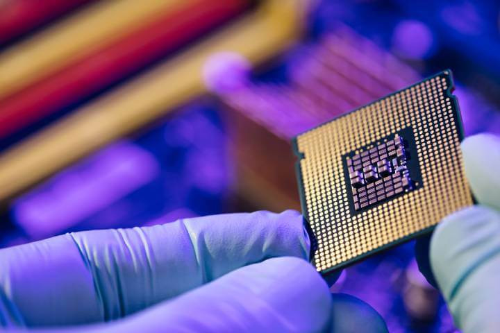 Visible silicon core and cache chip in a microprocessor.
Table of Contents:
- Why Semiconductors are the Backbone of Microchips
- The Rise of Silicon
- Exploring Alternative Semiconductor Materials Beyond Silicon
- Silicon Carbide: A Rising Star in Semiconductor Materials
- Gallium Nitride: A Game-Changer in Semiconductor Technology
- Packaging: Protecting and Connecting Semiconductors
- Challenges in Selecting Semiconductor Materials
- Environmental Impact of Semiconductor Materials
- Recycling Challenges of Semiconductor Materials
- Conclusion
Before diving deeper into the world of microchips, it's essential to address a fundamental question: What are microchips made of? At their core, microchips are composed of semiconductor materials, primarily silicon, which form the basis of their functionality.
At the heart of these indispensable components are semiconductors, materials that are fundamental to the operation of microchips. This article aims to explore the composition of microchips, shedding light on why these materials are crucial. By understanding what microchips are made of, we gain insight into the very fabric of our digital era's technology.
To gain a more comprehensive perspective on microchips, consider delving into the history of the microchip. This exploration traces the remarkable journey from the earliest prototypes to the advanced chips used today, providing valuable context to the evolution and impact of this technology.
Why Semiconductors are the Backbone of Microchips
What are microchips made of? The answer lies in semiconductors, the fundamental components that form the backbone of every microchip. These materials' unique electrical properties are what enable microchips to perform their critical functions in various electronic devices.
Semiconductors form the very foundation of microchips, playing a pivotal role in their functionality. Unlike conductors and insulators, semiconductors are partial conductors whose electrical properties can be adjusted with the use of doping (the inclusion of positively and negatively charged atoms). This unique characteristic of semiconductors allows them to form active components, such as transistors, which are crucial for controlling the flow of electrical current.
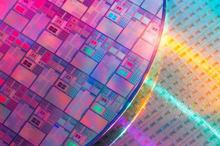
Silicon Wafers and Microcircuits with Automation system control application
While there are numerous semiconductor materials available, only a select few have proven to be practical for use in microchips. This is due to the stringent requirements for purity and specific electrical properties needed for effective semiconductor performance. The choice of semiconductor material can significantly impact the efficiency, speed, and power consumption of a microchip, making the selection process a key aspect of microchip design.
For those interested in a deeper dive into the manufacturing process of these intricate components, our previous article titled "How Microchips Are Made" offers a comprehensive look. It explores the intricate steps involved in transforming these semiconductor materials into the microchips that power our electronic world. Understanding the manufacturing process provides a fuller appreciation of the complexity and precision required to produce these vital components of modern technology.
The Rise of Silicon in the Semiconductor Industry
Exploring the ascendancy of silicon in the semiconductor industry reveals why this element has become the backbone of modern electronics.
Silicon's Electrical Superiority and Thermal Resilience
Understanding what computer chips are made of leads us directly to silicon. This material's optimal balance between conductivity and insulation sets it apart, making it the preferred choice for microchips.However, it is not just that silicon has ideal electrical properties but that its electrical properties can be changed with relative ease compared to other semiconductors. While there are other semiconductors that have superior characteristics, silicon is one of the few semiconductors that offers excellent trade-offs between power capabilities, maximum switching speed, and reliability.
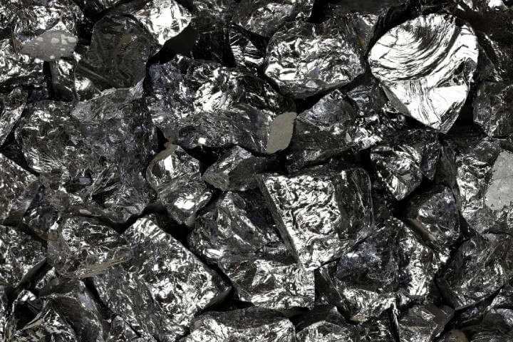
High-purity polycrystalline silicon sourced from Freiberg, Germany.
Thermal Resilience
Another significant advantage of silicon is its thermal properties. Silicon microchips can reliably operate in a variety of environmental conditions, enduring both high and low temperatures. This makes them ideal for use in a diverse array of applications, from automotive electronics, which must withstand extreme temperature fluctuations, to consumer electronics, which often operate in more controlled environments.
Abundance and Environmental Considerations of Silicon
The third factor contributing to silicon's dominance is its abundance. As silicon is one of the most plentiful elements on Earth, this abundance ensures a steady and scalable supply, a crucial factor for an industry that demands high volumes of raw material. The ready availability of silicon also makes it a cost-effective choice for mass production of microchips through economies of scale.
Environmental Considerations
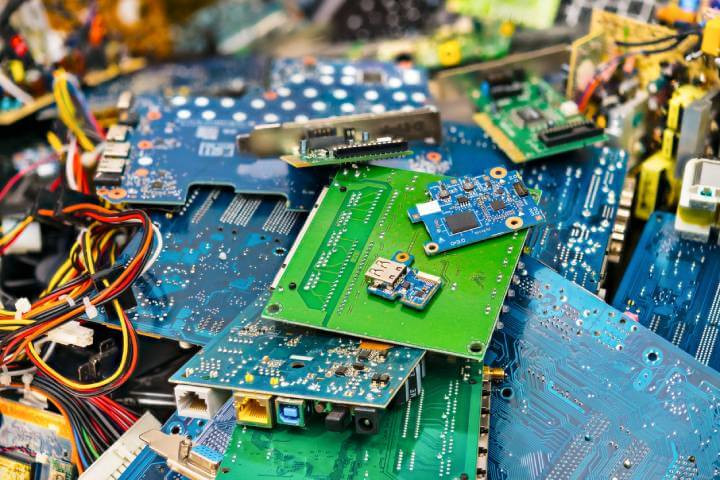 Colorful blur of PC components – connectors, PCBs, notebook cards, mainboards, integrated circuit boards, UTP, USB.
Lastly, the environmental impact of mining silicon is relatively minimal, especially when compared to other semiconductor materials. Extracting silicon from sand is a process that, while energy-intensive, does not involve the same level of environmental degradation or toxic byproduct generation as the mining of some other elements. This aspect is increasingly important in an era where sustainability and environmental impact are critical considerations for industries worldwide.
In summary, silicon's rise to prominence in the semiconductor industry is underpinned by its excellent electrical and thermal properties, its abundant availability, and its relatively low environmental impact. These factors combined have made silicon the material of choice for microchip manufacturers, shaping the landscape of modern electronics.
Exploring Alternative Semiconductor Materials Beyond Silicon
While silicon reigns supreme in the semiconductor industry, it's not the only material on the stage. There are specific applications where alternative semiconductor materials are not just beneficial but necessary.
In answering the question of what microchips are made out of, we find that beyond silicon, materials like Indium Gallium Nitride and Aluminium Gallium Indium Phosphide play a crucial role in specific applications such as LED manufacturing.
The Case of LEDs: Materials Beyond Silicon
A prime example of an application requiring different semiconductor materials is in the manufacturing of Light Emitting Diodes (LEDs). The fundamental principle behind LEDs is that as excited electrons fall back into lower energy states, they emit light. While silicon is immensely beneficial in integrated circuits, when it comes to LEDs, it is not suitable for this purpose as the energy levels in silicon cannot produce visible light (primarily emitting infrared photons, which are invisible to the human eye).
Despite their ubiquitous presence, the intricate workings of LEDs remain a mystery to many. This video demystifies the process, delving into the molecular interactions that allow electrons to emit photons and create light. It also sheds light on how scientists and engineers harness these principles to produce specific colours and package semiconductor material for practical use. Whether you're a budding electronics enthusiast or simply curious about the science behind everyday technology, this video offers a comprehensive and accessible exploration of LED technology.
For the creation of visible light LEDs, different materials are used:
- Indium Gallium Nitride (InGaN): This material is crucial for producing blue and green LEDs, which are critical for numerous applications including displays and lasers.
- Aluminium Gallium Indium Phosphide (AlGaInP): This material is used for red, yellow, and orange LEDs. Its unique properties allow for efficient photon emission in these colour ranges, making it a key material in the LED industry ranging from displays to indicators.

Hi-Res Images of Chemical Elements, CC BY 3.0, via Wikimedia Commons
Germanium: A Versatile Player in RF Applications
Another noteworthy semiconductor material is Germanium. While it may not be as widely used as silicon, Germanium has carved out its niche, particularly in Radio Frequency (RF) applications. Its properties make it highly effective in RF diodes, which are essential components in various communication and signal processing devices.
Summary of Alternative Semiconductor Materials
In summary, while silicon is the most popular choice for semiconductor applications, the world of semiconductor materials is rich and varied. Materials like Indium Gallium Nitride and Aluminium Gallium Indium Phosphide play critical roles in the LED industry, while Germanium finds its importance in RF applications. These alternative materials highlight the adaptability and diversity of semiconductor technology, catering to specific needs that silicon alone cannot fulfil. Understanding these alternatives opens up a window into the intricate and colourful world of semiconductor applications beyond the silicon horizon.
Silicon Carbide: A Rising Star in Semiconductor Materials
While silicon and silicon carbide aren't metals, addressing what metal microchips are made of brings us to the use of metalloid elements in semiconductor technology. These elements, including silicon, possess metal-like characteristics crucial for the functionality of microchips.
 An uncommon mineral stone - Silicon Carbide Moissanite
Advantages of Silicon Carbide
Silicon Carbide (SiC) is garnering significant attention as a semiconductor material poised to play a pivotal role in the future of electronics. Its unique properties offer substantial improvements over traditional silicon, particularly in applications where efficiency and high performance are paramount.
This engaging presentation takes you through the intricate processes involved in creating these tiny yet powerful components that are the heart of modern electronic devices. From the precision engineering of silicon wafers to the complex assembly of semiconductor layers, this video provides a comprehensive look at the technological marvels behind the microchips. Whether you're a tech enthusiast or simply curious about how these essential components are made, this video is a must-watch to appreciate the innovation and expertise driving the semiconductor industry.
Superior Thermal Conductivity
One of the standout features of Silicon Carbide is its exceptional thermal conductivity. This property allows SiC-based devices to operate effectively at much higher temperatures compared to their silicon counterparts. The ability to withstand elevated temperatures not only expands the range of applications but also enhances the reliability and lifespan of the devices.
Enhanced Electrical Conductivity
In addition to its thermal advantages, Silicon Carbide boasts a much higher electrical conductivity than silicon. This means that SiC devices can handle significantly more current for a given size, which is crucial in high-power applications. The increased conductivity also translates to reduced energy losses, making SiC an attractive option for applications where energy efficiency is a key concern.
Compact and Efficient Design
The inherent properties of Silicon Carbide allow for the creation of smaller devices compared to those made with silicon. This reduction in size is a significant advantage, especially in space-constrained applications. The ability to pack more power into a smaller package opens up new possibilities in electronic design and engineering.
Ideal for Power Amplifiers and EV Industry
Silicon Carbide's characteristics make it an ideal choice for power amplifiers, where efficiency and performance are critical. Its ability to handle high currents and operate at elevated temperatures without degradation is particularly beneficial in these applications.
Transformative Potential in EV and Green Energy
The potential of Silicon Carbide extends to industries like electric vehicles (EV) and green energy. In EVs, SiC can contribute to more efficient power conversion systems, leading to longer battery life and extended range. In the realm of green energy, SiC's efficiency and high-temperature tolerance make it well-suited for solar inverters and other renewable energy applications.
Summary: Silicon Carbide's Bright Future
In conclusion, Silicon Carbide is emerging as a highly promising semiconductor material, offering advantages in thermal and electrical conductivity, compactness, and efficiency. Its potential to revolutionise industries such as EV and green energy underscores its importance in the next wave of technological advancements. As we look to the future, Silicon Carbide stands out as a material that could redefine the boundaries of semiconductor applications, pushing the limits of what's possible in electronic design and energy efficiency.
Gallium Nitride: A Game-Changer in Semiconductor Technology
The Advantages of Gallium Nitride Over Silicon
Gallium Nitride (GaN) is emerging as a formidable contender in the semiconductor industry, boasting characteristics that significantly outperform traditional silicon. This material is capturing the attention of engineers and researchers worldwide, thanks to its superior properties that open up new possibilities in electronic design.
In a compelling segment from Electronica 2022, Electropages' Robin Mitchell engages in an enlightening conversation with Peter Comiskey, Director of Application Engineering at Cambridge Devices. This interview delves into the innovative realm of GaN (Gallium Nitride) devices, exploring the pioneering efforts of this start-up in the field. The discussion also ventures into the future, envisioning the energy-efficient landscape of the city in 2050 and the pivotal role GaN technology is poised to play. Additionally, unique features and contributions of Cambridge Devices in this emerging sector are highlighted. Tune into this insightful interview for an in-depth understanding of GaN’s potential and Cambridge Devices' vision for the future of energy efficiency.
Higher Bandgap: Enabling Greater Voltages
One of the key advantages of Gallium Nitride is its higher bandgap compared to silicon. This higher bandgap allows GaN-based devices to operate at greater voltages, a crucial factor for power electronics. The ability to handle higher voltages without breakdown enhances the performance and efficiency of electronic devices, making GaN an attractive material for a range of applications.
Faster Switching Capabilities
Another remarkable feature of GaN is its ability to switch much faster than silicon. This rapid switching capability is essential in high-frequency applications, where speed and efficiency are paramount. Faster switching not only improves performance but also contributes to energy savings, as devices can operate more efficiently with less power loss.
Thermal Considerations
While GaN offers many advantages, it does have lower thermal capabilities compared to Silicon Carbide. This means that while GaN can handle higher voltages and switch faster, it may not perform as well in extremely high-temperature environments. However, this limitation does not detract from its usefulness in a wide range of applications.
Ideal for RF Amplifiers and High-Frequency Applications
The properties of Gallium Nitride also make it particularly well-suited for RF amplifiers and other high-frequency applications. In these scenarios, the high bandgap and fast switching capabilities of GaN can be fully leveraged, leading to superior performance compared to silicon-based devices.
Summary: The Promising Future of Gallium Nitride
In summary, Gallium Nitride stands out as a future material with the potential to transform the semiconductor industry. Its higher bandgap, faster switching capabilities, and suitability for high-frequency applications position GaN as a highly promising alternative to silicon. As research and development in GaN continue to advance, we can expect to see this material play an increasingly important role in shaping the future of electronics, particularly in areas where high voltage and high-speed operation are critical.
Packaging: Protecting and Connecting Semiconductors
Delving into what computer chips are made up of extends beyond their semiconductor components. The packaging process, involving materials like plastic epoxy and ceramic, plays a vital role in protecting these delicate chips and ensuring their effective integration into electronic devices.
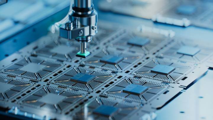 Process of Packaging Semiconductors
The Necessity of Semiconductor Packaging
Semiconductors, with their intricate and delicate structures, require robust packaging solutions. These packages not only protect the semiconductor's sensitive features but also facilitate connections to external circuits, ensuring functionality and reliability in various applications.
Chip-on-Board Technology
One prevalent method of packaging is the Chip-on-Board (CoB) technique. In this approach, semiconductor dies are directly attached to printed circuit boards (PCBs), and connections are made between the PCB and chip via gold wires, which are known for their excellent conductivity and reliability. Finally, the entire assembly is then secured and protected with a small amount of black epoxy. This method is particularly well-suited for mass production of basic electronic products, such as digital clocks, and peripherals like mouse and keyboards, where cost-effectiveness and compact design are key considerations.
IC Packages for Versatility
For semiconductors intended for more versatile applications, Integrated Circuit (IC) packages are commonly used. These packages come in various materials, each serving different needs:
- Plastic Epoxy Packages: Ideal for low-cost ICs, plastic epoxy packages are widely used due to their cost-effectiveness and adequate protection for general applications.
- Ceramic IC Packages: Suited for high-temperature and precision applications, ceramic packages offer superior thermal and chemical stability, making them suitable for more demanding environments.
Both plastic and ceramic packages typically incorporate a lead frame, which plays a crucial role in connecting the external pins of the chip to its internal contacts. However, the lead frame doesn't make direct contact with the chip, and instead uses gold wires, which are bonded to both the chip and the lead frame using ultrasonic welding. This method ensures a secure and reliable connection, crucial for the chip's performance.
The following video offers a practical glimpse into the intricate process of wire bonding, an essential step in microchip assembly. It demonstrates the precision required in connecting integrated circuits, a key technique in the functionality of various electronic devices. For those intrigued by the detailed craftsmanship behind microchip technology, this video serves as an excellent visual guide.
Advanced Solutions for High-Performance Chips
For high-performance chips, such as those found in CPUs and other high-speed digital systems, more advanced packaging solutions are employed. These often involve mounting the chips onto substrate boards, which are then enclosed in metal cans. This type of enclosure is particularly effective for heat dissipation, a critical factor in maintaining the performance and longevity of high-speed, high-power semiconductors.
Summary: The Art and Science of Semiconductor Packaging
In summary, semiconductor packaging is a critical aspect of chip design and manufacturing, encompassing a range of techniques from Chip-on-Board to advanced metal can enclosures. The choice of packaging is dictated by the application's requirements, balancing factors like cost, thermal management, and environmental resilience. As semiconductor technology continues to advance, the evolution of packaging solutions remains a key area of innovation, ensuring that these tiny yet powerful components can reliably function in an ever-expanding array of devices and systems.
Challenges in Selecting Semiconductor Materials
Selecting the right semiconductor material is a complex process, influenced by a multitude of factors. Each aspect plays a crucial role in determining the suitability of a material for a specific application, thus, understanding these challenges is key to making informed decisions in semiconductor design and manufacturing.
- Electrical Properties
The electrical properties of a semiconductor material are fundamental to its functionality, with such properties including bandgap, carrier mobility, and intrinsic conductivity. The choice of material directly impacts the efficiency, speed, and power consumption of the resulting semiconductor device. For instance, materials with a wider bandgap, like Silicon Carbide and Gallium Nitride, are preferred for high-voltage applications, while smaller bandgap semiconductors such as silicon are easier to work with and great for large-scale integrated designs.
- Mechanical Properties
The mechanical strength and durability of a semiconductor material are also vital, especially for devices subjected to physical stress or harsh environments. The material must withstand both fabrication processes and end-application environments while also maintaining integrity over the product's lifespan. As such factors like hardness, brittleness, and resistance to wear and tear should always be considered.
- Thermal Properties
Thermal management is a critical aspect of semiconductor design as semiconductors are greatly affected by temperature. Thus, semiconductors used in electronics must be able to dissipate heat effectively to prevent overheating and ensure reliable operation. Materials with higher thermal conductivity, like Silicon Carbide, are advantageous in high-power or high-temperature applications as they can readily remove heat, allowing for a more compact design.
- Material Cost
Cost is always a significant consideration when selecting a semiconductor material. The material should be economically viable for the intended application, especially for mass-produced items. While some materials may offer superior properties, their high cost can be a limiting factor, which is why silicon, being abundant and relatively inexpensive, remains a popular choice.
- Material Availability
The availability of the material is also closely tied to cost, with materials that are rare or difficult to extract and process not being feasible for large-scale production. As such, the semiconductor industry often favours materials that are readily available and sustainable over the long term.
Summary: A Balancing Act in Material Selection
In conclusion, selecting semiconductor materials is a balancing act that requires careful consideration of electrical, mechanical, and thermal properties, along with cost, availability, and production scale. Each factor plays a critical role in determining the overall performance and feasibility of the semiconductor device. As technology advances, new materials and alloys are continually being explored to meet the evolving demands of the semiconductor industry, making this an ongoing challenge for engineers and researchers.
Environmental Impact of Semiconductor Materials: Challenges and Concerns
The semiconductor industry, while pivotal to technological advancement, faces significant environmental challenges. The process of extracting and refining semiconductor materials, along with the manufacturing of semiconductor devices, has considerable environmental implications.
Energy Intensive Extraction and Refinement
While semiconductor materials like silicon are relatively abundant and easy to mine, extracting them from their ores is an energy-intensive process. The refinement of these materials to the purity levels required for semiconductor manufacturing demands significant energy input, often resulting in a substantial carbon footprint. This high energy requirement contributes to the overall environmental impact of the semiconductor industry.
Massive Water and Resource Consumption
Semiconductor manufacturing is also a resource-intensive process, particularly in terms of water usage. The production of a single semiconductor chip can require vast amounts of ultra-pure water, which not only strains local water resources, but also leads to challenges in water management and recycling within the manufacturing facilities.
Carbon Emissions
The energy-intensive nature of semiconductor manufacturing, especially in facilities powered by fossil fuels, leads to considerable CO2 emissions. As the demand for semiconductors grows, so does the concern over the carbon footprint of their production, prompting the industry to seek more sustainable and energy-efficient manufacturing processes.
Use of Hazardous Chemicals
The production of semiconductors involves various chemicals, many of which are toxic and harmful to both humans and the environment. These chemicals are used in processes like etching and cleaning of semiconductor wafers, and if not managed properly, carry a significant risk to the environment, causing contamination and damage to ecosystems.
Environmental Risks and Mitigation
Unchecked, these environmental concerns pose significant risks, however, the semiconductor industry is increasingly aware of its environmental responsibilities. Efforts are being made to reduce energy consumption, minimise water usage, lower carbon emissions, and manage chemical waste more effectively. Innovations in manufacturing technology and a shift towards renewable energy sources are part of the industry's response to these environmental challenges.
Quantum Computing: The Next Frontier in Chip Materials
Another innovative area in semiconductor technology is quantum computing. What are quantum computer chips made of? These chips use materials like superconducting circuits and silicon quantum dots, which allow for the creation and manipulation of qubits. Qubits, unlike traditional bits, enable quantum chips to process complex computations at speeds unattainable by conventional microchips, paving the way for groundbreaking advancements in computing.
Summary: The Environmental Equation in Semiconductor Manufacturing
In summary, while semiconductor materials are crucial for technological progress, their environmental impact cannot be overlooked. The industry faces the dual challenge of meeting the growing demand for semiconductors while also addressing the environmental concerns associated with their production. Balancing technological advancement with environmental responsibility is a key issue that the semiconductor industry continues to navigate, striving for more sustainable and eco-friendly manufacturing practices.
Recycling Challenges of Semiconductor Materials
The recycling of semiconductor materials presents significant challenges, stemming from their complex composition and integration into electronic devices. These challenges not only impact the feasibility of recycling but also raise additional environmental concerns.
Difficulty in Extraction and Reuse
One of the primary difficulties in recycling semiconductors is the extraction of components from electronic circuits. Once integrated into devices, semiconductors are often inseparable from other materials, making it challenging to extract them for reuse. Additionally, the process of disassembling and extracting these components can be labour-intensive and cost-prohibitive. Unlike other materials like glass or metal, semiconductor components cannot be reliably taken out and reused in new products without compromising their functionality and efficiency.
Presence of Toxic Compounds
Semiconductors are composed of numerous materials, some of which are toxic. These include heavy metals that are integral to the functionality of the semiconductor, but pose significant risks if not handled properly. The presence of these toxic substances complicates the recycling process, requiring specialised handling and disposal methods to prevent environmental contamination.
Environmental Risks of Improper Disposal
If semiconductor materials are not disposed of correctly, they pose a significant environmental hazard. When placed in landfills, these materials can leach toxic chemicals over time, and this leaching process can go on to pollute water sources, harm wildlife, and impede plant growth. The long-term environmental impact of such contamination can be profound, affecting ecosystems and potentially posing health risks to humans.
The Need for Sustainable Solutions
Given these challenges, there is a growing need for sustainable solutions in the semiconductor industry. This includes developing more eco-friendly materials, improving recycling technologies, and implementing responsible disposal practices. The industry is also exploring ways to design semiconductors and electronic devices with recycling in mind, aiming to make the end-of-life processing of these products more environmentally friendly.
Summary: Addressing the Recycling Dilemma
In conclusion, the recycling of semiconductor materials is fraught with challenges, from the difficulty of extraction and reuse to the environmental risks posed by toxic compounds. Addressing these issues is crucial for the semiconductor industry as it moves towards a more sustainable future. Innovations in material science, recycling technology, and product design are essential to overcome these challenges, ensuring that the benefits of semiconductor technology do not come at the expense of the environment.
Conclusion: Reflecting on the Semiconductor Landscape
As we conclude our exploration of semiconductor materials, it's clear that this field is as dynamic as it is complex. Silicon's long standing reign, challenged by innovative materials like Silicon Carbide and Gallium Nitride, illustrates the industry's constant evolution. These materials, each with their unique strengths and applications, from powering simple gadgets to enabling high-frequency operations, highlight the industry's diverse capabilities.
Yet, this technological advancement doesn't come without its share of challenges. The selection of semiconductor materials is a multifaceted decision, encompassing a range of factors from electrical efficiency to environmental impact. Moreover, the difficulties in recycling these materials remind us of the industry's significant environmental responsibilities.
Looking ahead, the semiconductor industry is poised at an exciting yet critical juncture. Balancing technological innovation with sustainable practices is more crucial than ever. As we continue to push the boundaries of what's possible in electronics, we must also forge paths toward more environmentally conscious methods. This balance is not just a goal but a necessity, ensuring that the semiconductor industry continues to thrive and innovate responsibly in the years to come.
