How are Microchips Made? From Silicon Crystals to Integrated Circuits
Educational | 30-11-2023 | By Robin Mitchell
Microchips, the cornerstone of modern electronics, are born from a process that is as intricate as it is fascinating. But how are microchips made? This article delves into the complex journey from silicon to sophisticated electronic components.
For a comprehensive understanding of this journey, it’s also valuable to explore the history of the microchip, tracing its origins and evolution over the years.
These diminutive components, which power everything from daily-use appliances to advanced computing systems, are the result of a highly sophisticated manufacturing process. This process, though complex, can be broadly categorised into three key stages: blank wafer production, fabrication, and encapsulation. Each stage is a marvel of engineering and science, reflecting the relentless pursuit of technological advancement.
Table of Contents:
- The Three Core Stages of Microchip Creation
- Wafer Growing: A Pivotal Step in Microchip Fabrication
- Wafer Fabrication: The Intricate Process of Crafting Microchips
- Encapsulation: The Final Stage in Microchip Manufacturing
- Challenges Faced in Microchip Fabrication: Navigating the Nanoscale
- Navigating the Future of Microchip Manufacturing
- Exploring Advanced Packaging in Microchip Manufacturing
- Who Makes Microchips?
- Conclusion
- References
- Frequently Asked Questions (FAQs)
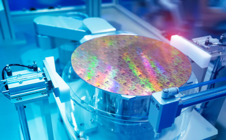
Advanced Automation in Action: Silicon Wafers and Microcircuits Under Precise System Control
This article not only explores how microchips are made but also provides insights into how a computer chip is made, from raw materials to the final product. The question of how micro chips are made leads us into the fascinating world of microchip manufacturing.
The Three Core Stages of Microchip Creation
Before diving into the specifics of microchip creation, it's essential to understand its three core stages. Each stage plays a pivotal role in transforming a simple silicon element into a complex and functional microchip.
Blank Wafer Production: The genesis of a microchip lies in the production of blank wafers. These wafers, primarily made from silicon due to its excellent semiconductor properties, serve as the foundation for microchip construction. The process begins with the meticulous growth of silicon crystals, which are subsequently sliced into thin, polished discs. This initial stage is crucial as it lays the groundwork for the intricate layers and structures that will be added later.
Fabrication: Following the creation of the blank wafers, the fabrication stage takes over. This is where the true magic happens. Through a series of highly controlled processes, including photolithography, doping, etching, and deposition, intricate circuits are imprinted onto the wafer. Each step in this phase requires absolute precision and control, as the smallest error can render the chip defective. The fabrication process is not just a testament to human precision but also to the advancements in nanotechnology and material science.
Encapsulation: The final stage in the journey of a microchip is encapsulation. After the wafer is fabricated with countless microscopic circuits, it needs protection. Encapsulation involves encasing the delicate structures in a protective material, safeguarding them from physical damage and environmental factors. This stage is critical for ensuring the longevity and reliability of the microchip, especially considering the extreme conditions they often operate under.
Having established the overarching framework of microchip manufacturing in the introduction, we now delve into the first critical phase of this intricate process: Wafer Growing.
Wafer Growing: A Pivotal Step in Microchip Fabrication
Wafer growing plays a pivotal role in the fabrication of microchips, embodying a perfect blend of precision and scientific acumen. This process is crucial as it sets the stage for embedding thousands of devices onto a single wafer, thereby streamlining the manufacturing process and harnessing economies of scale to reduce overall costs. Let’s delve into the nuanced steps of wafer growing, a process that is as much an art as it is a science in the realm of semiconductor production.
The process of how silicon chips are made begins with the pivotal step of wafer growing, particularly, using the Czochralski method.
The Czochralski Method: The Art of Crafting Silicon Wafers
In exploring how a silicon chip is made, the Czochralski method stands out as a fundamental technique.
- Initiating the Process: The journey of wafer creation begins with the Czochralski Method, a technique that has been a staple in silicon wafer production for over a century. This method involves the use of a small, meticulously chosen seed crystal of pure silicon.
- The Crucial Dip and Draw: The seed crystal is delicately dipped into a molten vat of silicon. As it is slowly drawn out, it is simultaneously rotated. This rotation, coupled with the careful upward motion, is critical for the growth process.
- Introducing Impurities for Semiconductor Types: To tailor the semiconductor properties of the silicon, specific impurities, known as dopants, are added to the molten silicon. Elements like Boron and Phosphorus are commonly used to create either p-type or n-type semiconductors, each with distinct electrical properties essential for various microchip functions.
- Uniform Crystal Growth: As the seed crystal is withdrawn from the molten vat, a large, uniform cylinder of silicon, known as an ingot, forms beneath it. The Czochralski Method ensures that this ingot is a single crystal, free from imperfections. This uniformity is not just a matter of structural integrity; it is vital for the semiconductor’s functionality, as the effectiveness of a microchip hinges on the purity and flawlessness of the crystal.
- From Ingot to Wafer: Once the single-crystal silicon ingot is fully grown, it undergoes a cooling process. The next step is slicing this ingot into thin, large wafers using high-precision diamond blades. The diameter of these wafers can vary, typically ranging from 100mm to 300mm, depending on the requirements of the microchip being produced.
The meticulous process of growing and preparing silicon wafers sets the stage for the next critical phase in microchip production: wafer fabrication. This next step in the journey of microchip creation is where the carefully prepared wafers undergo a transformation.
Visualising the Czochralski Method: Silicon Ingot Growth Animation
To complement the detailed explanation of the Czochralski Method in the article, the following video provides a vivid animation of silicon ingot growth inside an LCT furnace. This visual aid, presented by Linton Crystal Technologies, offers an insightful glimpse into the intricate process of growing silicon crystals, a fundamental step in microchip production. Watch the animation to see the theoretical aspects of the Czochralski Method come to life.
Wafer Fabrication: The Intricate Process of Crafting Microchips
The journey of microchip manufacturing continues with wafer fabrication, a stage where semiconductor foundries transform the pristine silicon wafers into complex electronic devices. This phase is a meticulous blend of chemistry, physics, and nanotechnology, involving multiple steps to build up individual layers on the silicon wafer.
Delving deeper into how a semiconductor chip is made, we will explore the detailed steps involved in wafer fabrication. This section provides a detailed look into how electronic chips are made, focusing on the wafer fabrication process.
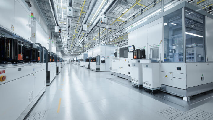
A wide shot of the cleanroom in a semiconductor fabrication facility, showcasing the sophisticated overhead wafer transfer system in action.
The Detailed Steps of Wafer Fabrication
The intricate process of how semiconductor chips are made involves multiple cycles of layering, patterning, and etching.
- Preparation and Orientation: The process begins with the thorough cleaning of the wafers, preparing them for the intricate fabrication process. Correct orientation is crucial at this stage due to the wafers’ crystalline structure, which must be aligned precisely for the subsequent steps.
- Oxide Layer Growth: The first step in the layering process involves growing an oxide layer on top of the wafer. This layer plays a vital role in controlling the doping process, which is essential for altering the electrical properties of the semiconductor.
- Photoresist Application and UV Imaging: A layer of photoresist, a light-sensitive material, is then applied to the wafer. The image of the doped regions is projected onto the photoresist using ultraviolet (UV) light. This step is critical for defining the intricate patterns of the microchip’s circuits.
- Development and Etching: After exposure to UV light, the photoresist is developed, removing the unexposed areas. A strong acid, such as Hydrofluoric acid, is then applied to etch away the oxide areas not protected by the photoresist.
- Doping Process: Dopants are introduced to the semiconductor at this stage. The areas not covered by photoresist absorb these dopants, altering their electrical properties to create N and P type regions, which are fundamental for transistor functionality.
- Additional Oxide Layer and Gate Formation: Another oxide layer is grown over the entire wafer, serving as the foundation for transistor gates. A new layer of photoresist is applied, and the gate structure is imaged onto the wafer using UV light. The subsequent development and etching process creates the semiconductor regions that form the transistors.
- Interconnect Fabrication: The final stage involves the fabrication of interconnects, which link the various semiconductor regions. Unlike oxide layers, interconnect layers are made from metals like aluminum, deposited using vacuum deposition techniques. These metal layers are then patterned with resist and etched, similar to the earlier steps.
- Layering and Patterning: The process of layering, applying photoresist, developing, and etching is repeated to create the interconnects. A chip can have as many as 15 interconnect layers, although designers typically aim for between 3 and 6 layers to balance complexity and functionality.
Wafer fabrication stands as a testament to the complexity and precision inherent in microchip manufacturing. It’s in this phase that a simple silicon wafer undergoes a remarkable transformation into a microchip. This process isn’t just a single step but a series of multiple cycles involving layering, patterning, and etching. Each of these steps is meticulously executed, building up the microscopic structures that eventually define the microchip.
The fabrication process transcends mere imprinting of designs onto silicon. It’s akin to a symphony of advanced technological processes, each playing a crucial role. From the careful application of photoresist to the precision of the final etching, every action demands not only exact control but also a deep understanding of material properties and semiconductor physics.
Exploring Microchip Manufacturing: A Deep Dive with Sam Zeloof
The YouTube video titled "Z2 - Upgraded Homemade Silicon Chips" by Sam Zeloof showcases the fascinating process of creating silicon chips at home. Zeloof delves into the intricate world of semiconductor fabrication, demonstrating how a simple rock can be transformed into a computer chip through a series of chemical treatments. This video offers a unique perspective on the microchip manufacturing process, highlighting the creativity and ingenuity involved in producing these essential components of modern technology.
His hands-on approach and innovative techniques provide a captivating glimpse into the complexities and wonders of semiconductor fabrication.
As this stage concludes, what was once a plain silicon wafer emerges as a complex labyrinth of electronic circuits. These circuits, intricately designed, are now ready to embark on the next crucial phase of their journey: encapsulation.
- Jiang, H., & Yih, Y. (2019). Wafer Fabrication: Equipment and Productivity. In Semiconductor Manufacturing Handbook (2nd ed.). Elsevier. Retrieved from https://www.sciencedirect.com/science/article/abs/pii/S027861251930024X[1]
Encapsulation: The Final Stage in Microchip Manufacturing
After understanding how semiconductor chips are made through the fabrication process, the encapsulation stage is the next crucial step. The final steps in how a semiconductor chip is made involve the intricate process of encapsulation and testing.
Encapsulation marks the final stage in the journey of microchip production, a phase where the completed wafers are prepared for real-world application. This stage is as crucial as the earlier phases, involving a series of precise and delicate processes to ensure that each microchip is functional, protected, and ready for integration into electronic devices.
The encapsulation process is a key stage in understanding how IC chips are made, ensuring the protection and functionality of the microchips.
The Detailed Steps of Encapsulation
- Individual Testing with Wafer Prober: Once the wafer fabrication is complete, each device on the wafer undergoes rigorous testing. This is done using a specialised jig known as a wafer prober. The wafer prober rapidly makes contact with each device, injects test signals, and records the results. This step is vital to ensure that each microchip meets the required performance standards.
- Marking and Discarding Defective Devices: Devices that fail the testing phase are marked with a dot. These marked devices are eventually discarded, as they do not meet the stringent quality and performance criteria necessary for reliable functioning.
- Die Preparation and Slicing: The next step involves preparing the wafer die. This process begins with slicing the wafer into individual dies using a precision diamond saw. This slicing must be done with great care to avoid damaging the delicate structures on each die.
- Placement into IC Packages: After slicing, the wafer dies are carefully picked out from the wafer and placed into Integrated Circuit (IC) packages. This step is crucial as the IC package will protect the microchip from physical and environmental damage.
- Connecting Wafer to Packaging Pins: Once placed in the IC package, automated tools are used to connect the wafer to the packaging pins. This connection is made using tiny gold wires, which are bonded to the wafer and pins using ultrasonic welding. This method ensures a strong and reliable bond, essential for the microchip’s functionality.
- Sealing and Laser Etching: The final steps in the encapsulation process involve sealing the packages and then laser etching them with the manufacturer’s logo and other key details, such as the year of manufacture and the version of the chip. The sealing process protects the delicate internal components of the microchip, while the laser etching provides essential information about the chip for identification and tracking purposes.
The encapsulation stage in microchip manufacturing is characterised by its meticulous precision and attention to detail. It marks the final phase in the transformation of a simple silicon wafer into a sophisticated semiconductor device. This phase encompasses a series of critical steps, each vital to the integrity and functionality of the final product.
Firstly, each device on the wafer undergoes individual testing using a wafer prober. This step is essential to ensure that every microchip meets the required performance standards. Following this, devices that fail the testing phase are marked and subsequently discarded, as they do not meet the stringent quality criteria necessary for reliable functioning.
The process then moves to the precise slicing of the wafer into individual dies. This step requires great care to avoid damaging the delicate structures on each die. Once sliced, these dies are carefully placed into Integrated Circuit (IC) packages. This placement is crucial, as the IC package is responsible for protecting the microchip from physical and environmental damage.
Exploring Wire Bonding: A Key Step in Microchip Encapsulation
To further enhance our understanding of the microchip manufacturing process, particularly in the encapsulation stage, let's delve into a critical component: wire bonding. This process is essential for connecting the microchip to its packaging, ensuring functionality and protection. The following video, titled "Wire Bonding Basics - Manual Wedge Bonding ICs" from Sam Zeloof, offers an insightful look into this intricate process. It provides a practical perspective on how wire bonding is executed, highlighting its importance in the overall manufacturing journey of a microchip.
As we delve into microchip fabrication, the shift towards nanoscale technology brings forth significant challenges. The next section examines the intricate hurdles and innovative solutions in miniaturizing transistors, underscoring the delicate interplay between technological limits and breakthroughs.
Challenges Faced in Microchip Fabrication: Navigating the Nanoscale
The journey of microchip fabrication, while a marvel of modern engineering, is fraught with significant challenges, especially as the industry moves towards increasingly smaller transistors. These challenges are not just about scaling down sizes; they represent a fundamental shift in the way microchips are designed and manufactured.
Addressing the question of how is a semiconductor chip made, we explore the various challenges and innovations in the industry.
Overcoming the Hurdles of Miniaturization
- Transition from Micrometers to Nanometers: In the earlier days of microchip technology, features on chips were measured in micrometers. These sizes were manageable with traditional lithography techniques, using normal lenses and visible light. However, as the industry pushes towards nanometer-scale features, the fabrication process becomes exponentially more difficult.
- Advanced Lithography for Smaller Features: To create features in the nanometer range, engineers must employ extremely high-frequency ultraviolet (UV) light along with specialised lenses and advanced projection systems. This shift is not merely a matter of using more powerful equipment; it represents a significant technological leap.
- Dealing with Light Wavelength Limitations: A unique challenge arises when the wavelength of the light used in lithography is larger than the features being created. This necessitates the use of special diffraction patterns to achieve the desired precision, adding another layer of complexity to the fabrication process.
- Quantum Phenomena in Small Transistors: As transistors shrink, they become increasingly susceptible to quantum phenomena, such as quantum tunneling. This phenomenon can lead to electrons passing through barriers they traditionally wouldn’t, posing a significant challenge for maintaining the integrity and functionality of the microchip.
- Spacing Issues with Miniaturized Components: The reduction in size also makes it challenging to place wires and transistors close to each other without interference. This proximity can lead to unwanted interactions and crosstalk, complicating the design and functionality of the microchip.
The microchip industry’s relentless pursuit of miniaturization brings with it a host of complex challenges. Engineers and scientists are constantly pushing the boundaries, developing advanced lithography techniques to create ever-smaller components. This drive towards miniaturization isn’t just about shrinking sizes; it’s about mastering the intricacies of placing components in increasingly confined spaces.
One of the significant challenges in this endeavor is managing quantum phenomena. As components get smaller, quantum effects like tunneling become more pronounced, posing new hurdles in maintaining the integrity and functionality of microchips. Addressing these issues requires not only innovative solutions but also a profound understanding of both physical and quantum mechanics.
- Chou, J. C., Chen, K. H., Wang, J., & Huang, K. T. (2021). Challenges in Semiconductor Manufacturing under the Trend of Miniaturization. Journal of Microelectromechanical Systems, 30(1), 1-14. Retrieved from https://www.ncbi.nlm.nih.gov/pmc/articles/PMC7816552/[2]
Navigating the Future of Microchip Manufacturing
As the microchip industry evolves, it faces the challenge of surpassing the limits of traditional methods. The future of microchip manufacturing lies in groundbreaking technologies that promise to redefine the norms of semiconductor fabrication.
Exploring Beyond Traditional Lithography: The industry is investigating the potential of particle beams for direct carving into semiconductors. This method could bypass the limitations of traditional lithography, which becomes less feasible at extremely small scales.
Innovative Moulding Techniques: Direct moulding is another area of exploration. Here, features are grown on a stamp using non-lithographic methods and then transferred onto the wafer. This could enable more intricate designs at smaller scales.
New Semiconductor Materials: The search for alternative semiconductor materials is ongoing. These new materials might offer better performance or fabrication ease at smaller scales, potentially revolutionising microchip production.
Optical Computing: A significant shift under consideration is moving from electricity to light for data transmission within chips. Optical computing could bring substantial improvements in speed and energy efficiency.
Manufacturing in Space: Looking further ahead, there’s the possibility of manufacturing chips in space. The unique conditions of space – vacuum, solar energy, and microgravity – could offer distinct advantages in the manufacturing process.
The exploration of future technologies in microchip manufacturing signifies a pivotal shift in the industry. This shift is characterised by an unyielding drive towards innovation, particularly in overcoming the challenges associated with miniaturization. The sector is currently experiencing a surge in cutting-edge methodologies. These include advanced direct carving techniques, which allow for more precise and intricate designs, and the exploration of new semiconductor materials that promise enhanced performance and efficiency.
Another exciting frontier is the potential of light-based computing. This approach, still in its nascent stages, could revolutionise the way microchips process and transmit information. These developments are not mere incremental improvements; they represent a significant leap into a future where the conventional boundaries of microchip technology are being redefined.
- Yang, Z. (2023). What’s next for the chip industry. MIT Technology Review. Retrieved from https://www.technologyreview.com/2023/01/03/1065959/whats-next-chip-industry-2023/[3]
Exploring Advanced Packaging in Microchip Manufacturing
Applied Materials, Inc offers a narrated animation that illustrates the integration of logic chiplets and towering memory stacks. This advanced packaging is pivotal in driving significant improvements in system performance, reducing power consumption, and optimising size and cost. It's an insightful look into the innovative techniques that are redefining the boundaries of microchip technology.
Exploring the global landscape of microchip manufacturing, the next section highlights key nations and their strategic roles in the semiconductor industry.
Who Makes Microchips?
In the global arena of microchip manufacturing, the landscape is shaped by a few key nations, each contributing distinctively to the semiconductor industry. This field, marked by intricate technological prowess and strategic importance, sees various countries playing pivotal roles.
Taiwan emerges as a central figure in the production of advanced microchips. Its semiconductor foundries are among the world’s largest and most sophisticated, making it an indispensable player in the technology sector.
The Netherlands holds a crucial position, especially in the development of Extreme Ultraviolet (EUV) lithography. Dutch company ASML, a leading supplier of these advanced lithography machines, plays a vital role in enabling the production of the latest generation of microchips.
The United States is a key contributor in the realm of processors and high-end semiconductors. Housing some of the world’s leading semiconductor companies, the U.S. is at the forefront of innovation and advanced technologies in the microchip industry.
Japan and South Korea also hold significant roles, known for their expertise in various components and materials essential for microchip manufacturing. Their contributions are diverse, covering a broad spectrum of the production process.
China, navigating through international sanctions, has shown a persistent effort in the semiconductor sector. The dynamics between China and Western countries in this field reflect the strategic importance of microchip manufacturing in global politics and economics.
This global tapestry of microchip manufacturing is a testament to the field’s complexity and dynamism. It’s a landscape characterised by continuous technological advancements, geopolitical nuances, and strategic partnerships. As the demand for increasingly sophisticated and efficient microchips grows, the roles and interactions of these nations will continue to influence the trajectory of technology, impacting everything from consumer electronics to national security. The sector’s evolution and international collaborations highlight the pivotal role of microchips in our digitally-driven, interconnected world.
Conclusion
In conclusion, understanding how computer chips are made reveals the remarkable ingenuity and precision that define the semiconductor industry.
The global microchip manufacturing landscape is a complex and dynamic field, characterised by technological advancements, geopolitical influences, and strategic collaborations. Countries like Taiwan, the Netherlands, the United States, Japan, South Korea, and China each play crucial roles in different segments of the industry, from the production of basic components to the development of the most advanced semiconductor technologies.
As the demand for more sophisticated and efficient microchips continues to grow, the interplay between these nations will shape the future of technology, influencing everything from consumer electronics to national security. The ongoing advancements and global collaborations in this sector underscore the critical importance of microchips in our increasingly digital and interconnected world.
As we have seen, understanding how electronic chips are made involves a deep dive into the world of advanced manufacturing techniques.
References
- Jiang, H., & Yih, Y. (2019). Wafer Fabrication: Equipment and Productivity. In Semiconductor Manufacturing Handbook (Second Edition). Elsevier. https://www.sciencedirect.com/science/article/abs/pii/S027861251930024X
- Chou, J. C., Chen, K. H., Wang, J., & Huang, K. T. (2021). Challenges in Semiconductor Manufacturing under the Trend of Miniaturization. Journal of Microelectromechanical Systems, 30(1), 1-14. https://www.ncbi.nlm.nih.gov/pmc/articles/PMC7816552/
- Yang, Z. (2023). What’s next for the chip industry. MIT Technology Review. https://www.technologyreview.com/2023/01/03/1065959/whats-next-chip-industry-2023/
Frequently Asked Questions (FAQs)
How are microchips made so small?
Microchips are made incredibly small through advanced manufacturing techniques such as photolithography and etching. These processes allow for the creation of extremely tiny and precise circuits on silicon wafers, and the use of nanotechnology and ongoing advancements in semiconductor fabrication enable the production of progressively smaller microchips.
Who is the biggest chip manufacturer in the world?
The biggest chip manufacturer in the world is Taiwan Semiconductor Manufacturing Company (TSMC). Renowned for their cutting-edge manufacturing capabilities, TSMC produces chips for numerous leading technology companies globally.
How do you manufacture computer chips?
The manufacturing of computer chips involves a multi-step process. It begins with the production of silicon wafers, followed by intricate fabrication processes including photolithography, doping, etching, and deposition. The final stage is encapsulation, which protects the delicate circuits of the chip and allows it connect to external circuits.
How is silicon turned into computer chips?
Silicon is transformed into computer chips through a series of sophisticated processes. Initially, silicon is purified and crystallized, then sliced into thin wafers. These wafers undergo various fabrication stages, including doping, etching, and layering, to create the complex electronic circuits of a computer chip.
How long does it take to make 1 semiconductor chip?
The time to make a single semiconductor chip varies depending on the complexity of the chip and the manufacturing capacity. Generally, it can take several weeks from start to finish, considering the intricate processes involved in fabrication and testing.
What are the 8 steps of semiconductor manufacturing?
The 8 steps of semiconductor manufacturing typically include:
- Silicon purification.
- Crystal growth and wafer slicing.
- Wafer polishing.
- Photolithography.
- Etching.
- Doping.
- Metallization.
- Assembly and packaging
