Intel's Glass Substrate Breakthrough: The Future of Semiconductors?
In The News | 26-09-2023 | By Robin Mitchell
As the pressure to find new semiconductors continues to increase, researchers from Intel have recently revealed how their latest glass substrates will help Intel put one trillion transistors on a single die in the next few years. What challenges does silicon present as a semiconductor, what has Intel released, and is glass the next substrate for future semiconductors?
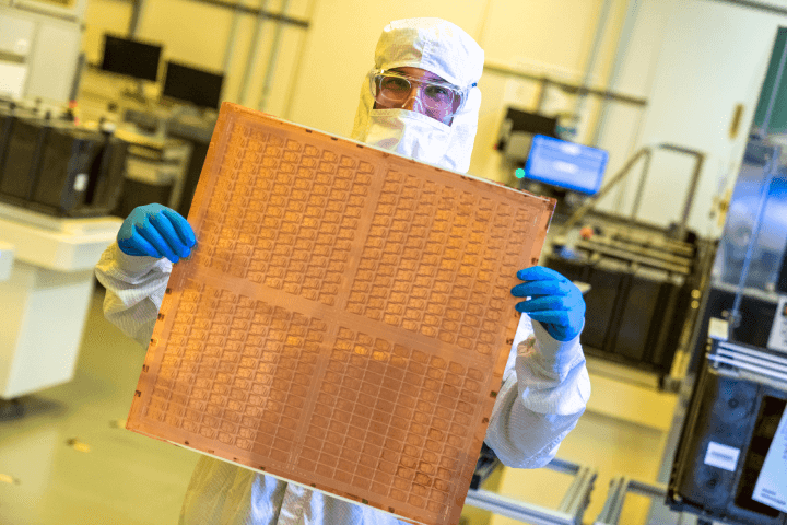
In July 2023, at Intel's Assembly and Test Technology Development facilities in Chandler, Arizona, an engineer from Intel is seen with a test panel made of glass core substrate. It is here at Intel's Assembly and Test Technology Development factories that Intel's cutting-edge packaging technologies are put into action. (Image courtesy: Intel Corporation)
What challenges does silicon present as a semiconductor?
Even though semiconductor manufacturers are able to continue shrinking the size of transistors, with 3nm devices just around the corner, the guideline “Moore’s Law”, which sees the number of transistors on chips doubling every two years, is slowing down (some have even said that it is no Moore). When considering that transistors are rapidly approaching the molecular scale, it makes complete sense that there will eventually be a physical limitation that will prevent transistors from being shrunk down anymore (no amount of new technology can fix this).
However, shrinking transistors is not the only option available to engineers when trying to increase transistor densities on chips. One other option that is being explored in this very instance is 3D chips, whereby chips have multiple active layers that can each house transistors. But getting this to work is not exactly trivial, with numerous issues ranging from layer deposition to imaging introducing all kinds of problems.
Technological Limitations and Quantum Effects
So, as 3D chips are not currently practical, what is it about current technology that prevents rapid shrinking? Well, there are numerous reasons for this…
To start, the size of features in transistors are becoming so small that they are far smaller than the wavelength of light used during exposure steps (see photolithography). As such, masks used to create such semiconductors are obscenely complex, and even more so in the machinery used to produce high-frequency UV light. In fact, the machinery needed to produce such UV light is so complex that only one company in the entire world, ASML, can produce them.
Another issue that semiconductors face is that as the feature sizes of transistors approach the atomic level, a high degree of precision is needed to accurately align layers. As semiconductors are manufactured one layer at a time, any misalignment will result in an entire wafer failing, and trying to match up masks on the nanometre scale can be a difficult task.
When it comes to the physical nature of materials, transistors that have nanometre-sized features are subject to quantum effects, which drastically alter their behaviour. For example, because modern transistors have extremely thin gates and channels, electrons can tunnel across insulative barriers in a phenomenon called quantum tunnelling. Such effects make it hard to reduce energy consumption, increase device speed, and even affect the switching performance of a transistor, giving it poor qualities.
Approaching the quantum scale has also introduced other challenges that have historically not been a major concern. For example, some materials (such as silicon) are not ideal for creating ultra-flat surfaces to grow transistors on. Such ultra-flat surfaces are needed to ensure that projections during photolithography are in focus, and any variation in the surface height can introduce image distortions.
Intel announces new glass substrate
To try and increase the number of transistors on a single package, Intel has developed numerous packaging technologies which combine multiple dies on a single substrate. These substrates provide interconnects between various dies, allowing for complex designs to be broken down into smaller devices, thus increasing wafer yields.
However, the current substrates used are generally organic in nature and made from similar materials found in PCBs. Such materials introduce a range of issues, including uneven surfaces, difficulty in forming bonds, and variation in characteristics.
Recognising these challenges, Intel has recently announced a new package substrate that it says will revolutionise the chiplet industry. The new substrate material is based on glass and has been in development for over a decade.
"After a decade of research, Intel has achieved industry-leading glass substrates for advanced packaging. We look forward to delivering these cutting-edge technologies that will benefit our key players and foundry customers for decades to come.”
–Babak Sabi, Intel senior vice president and general manager of Assembly and Test Development
Challenges and Advantages of Glass Substrates
While glass may be an everyday material, there are numerous factors that make it difficult to work with. For example, fibreglass-based materials can be laminated and layered with ease, while glass is a homogenous material, meaning that trying to embed multiple layers of interconnects is massively challenging. Another challenge that glass faces is that the chemicals used to etch it can often damage most materials (hydrofluoric is notorious for this).
And yet, Intel has managed to develop the technology to create chip substrates out of glass instead of woven fibreglass. But what advantages does such a substrate provide?
To start, glass has excellent thermal properties, and the thermal expansion of glass is very similar to silicon dies (thanks to both being made from silicon). This means that dies bonded to a glass substrate will expand and contract with the substrate, thereby reducing thermal stresses between the two materials.
Secondly, glass has better electrical insulative properties compared to fibreglass. This means that interconnects can be positioned much closer together and, thus, increase the signal density of packages. The use of glass substrates also introduces the possibility for optical channels, which would allow dies to directly communicate with optic systems (and thus, see massive gains in bandwidth).
Thirdly, the ability for glass to be extremely flat also introduces new lithography opportunities. As glass can be made extremely flat, projected designs can be made significantly smaller (as there is less surface variation). Thus, glass substrates can have far more through-hole connectors and incorporate smaller features.
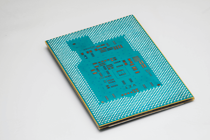 In a photograph taken in July 2023 at Intel's Assembly and Test Technology Development facilities in Chandler, Arizona, the ball grid array side of an Intel-assembled glass substrate test chip is visible. It's at Intel's Assembly and Test Technology Development factories where Intel's state-of-the-art packaging technologies are put into action. (Image credit: Intel Corporation)
While the new substrates are only in the testing phase, Intel expects that the new packages will be available by the end of the decade.
According to Intel's official announcement, the semiconductor industry will likely reach its limits on being able to scale transistors on a silicon package using organic materials by the end of the decade. This makes the development and implementation of glass substrates crucial for the next generation of semiconductors. Intel's research indicates that glass substrates can tolerate higher temperatures, offer 50% less pattern distortion, and have ultra-low flatness for improved depth of focus for lithography. As a result, a 10x increase in interconnect density is possible on glass substrates.
Will glass become the next substrate?
As engineers struggle to find new methods for reducing the size of transistors, alternative techniques will play a critical role in increasing device performance. The development of System on Modules, for example, has allowed engineers to split up complex designs into smaller units that can be combined on a single substrate.
In the case of Intel, it is clear that substrates currently being used will struggle to provide the performance of future devices, and glass will ultimately become the superior substrate for complex devices. In fact, it may be possible in the future for the substrate itself to integrate active components, such as level shifters, bus multiplexers, and power conditioning, to reduce the number of external components as well as allow bonded dies to focus more on computation.
For the time being, organic substrates will remain king in the field of packaging, but it may be sooner rather than later that glass starts to become a popular choice for future devices.
Intel's vision for the future is clear. As stated, "Intel is on the path to delivering 1 trillion transistors on a package by 2030 and its ongoing innovation in advanced packaging including glass substrates will help achieve this goal." This ambitious goal underscores the importance of continuous innovation in the semiconductor industry.
