Nanoscale Imaging Unlocks the Secret of Super-High-Frequency MEMS Resonators
Technical Analysis | 22-03-2023 | By Liam Critchley
Microelectromechanical system (MEMS) are gathering a lot of interest in a range of applications and are devices that are made up of both electrical and mechanical components. A number of device types can be created with MEMS spanning a number of application areas. One example of a popular MEMS device is a MEMS resonator, which convert electrical energy into a mechanical vibration through piezoelectric transducers.
These MEMS devices utilise elastic micrometre scale wavelengths in the GHz range and exhibit a high-quality factor (Q) and a low acoustic loss. Resonators with high-quality factors are ideal because they have low damping and vibrate for longer. In the super high frequency (3-30 GHz) regime, high-Q piezoelectric resonators are used in consumer electronics, scientific instruments, RF filter in wireless telecoms, and in quantum technologies.
MEMS resonators that utilise densely packed resonances are also sought after for multifrequency systems such as comb filters, reconfigurable oscillators, and multi-phonon quantum acoustic sources. However, the realisation of acoustic MEMS resonators for these applications relies on understanding the devices at the microscopic level to better understand the mechanical mode profiles, energy dissipation channels, spurious modes, and any imperfections that arise during microfabrication.
One of the main challenges is that a lot of imaging methods don’t have good enough spatial resolutions to image these different modes during the design process. This means that many of these features often get overlooked when MEMS resonator devices are designed and manufactured. Researchers have now chosen to utilise nanoscale imaging methods to better image a freestanding super-high-frequency lateral overtone bulk acoustic resonator.
Limitations of Current Techniques
To meet the demands of multifrequency system applications, it’s desirable to directly visualise the acoustic mode profiles at super high frequencies. This has typically proved challenging because acoustic wavelengths are on the order of 1 μm, so a spatial resolution of 100 nm or better is required to image these modes locally. Moreover, this is further complicated by the vibration amplitude dropping at high operation frequencies (due to a higher structure stiffness at smaller dimensions), and many acoustic modes in existing piezoelectric resonators have in-plane oscillations. Therefore, with these additional challenges to account for, the sensitivity of the imaging mode needs to be below 1 picometre (pm).
A number of microscopy methods―including those which are routinely used to characterise nanomaterials and thin films―have already been used for probing GHz scale acoustic fields, but all have been found to be limited in one way or another. For example, if you take scanning electron microscopy (SEM), acoustic imaging is limited to sub-GHz frequencies due to becoming charged (charging effect) from the electron beam.
On the other hand, atomic force microscopy (AFM) uses nonlinear effects to detect changes in a surface (at the nanoscale), but this approach is not useful for systems that have low signal levels. X-ray imaging is another method that’s been trialled, but the approach requires highly coherent X-ray sources, limiting its use and limiting its sensitivity.
There are also a number of laser-based imaging methods―such as interferometry―that have been used, but these optical methods have a diffraction-limited spatial resolution and only detect vertical displacement. The optical contrast is also usually too weak to be used with the transparent piezoelectric membranes used in super high-frequency resonators. Given the challenges associated with traditional imaging methods when it comes to super high-frequency MEMS resonators, researchers have been searching for other techniques with a high spatial resolution that are more suitable and can provide better and more accurate insights into the acoustic mode profiles of these devices.
Visualising Acoustic Waves with Nanoscale Imaging
Researchers have now been able to visualise acoustic waves in a freestanding super high-frequency freestanding LiNbO3 thin-film resonator using transmission-mode microwave impedance microscopy (TMIM). In this study, a lateral overtone bulk acoustic resonator (LOBAR) was used as the test bed with transducer electrodes only covering a small section of the acoustic cavity to excite the overtone response. The method was shown to have an excellent spatial resolution and a femtometre level of displacement sensitivity, making it suitable for imaging the individual overtones within the resonator.
LOBARs were chosen for the study because they are different to conventional resonators with low acoustic and thermoelastic damping. This is due to a smaller footprint of electrodes which increases the Q-factor for each of the overtones. The imaging approach taken mapped the piezoelectric potential in both real-space and reciprocal-space images and allowed the researchers to obtain direct information on the acoustic profile of individual tones, anchor leakage, and spurious transverse modes. The spatial resolution of these maps modes was on the order of 100nm, allowing the acoustic wavelength and phase velocity to be quantitatively deduced.
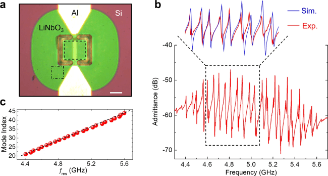
a Optical image of the LiNbO3 LOBAR, showing the aluminum electrodes, release window, suspended piezoelectric thin-film, and the silicon substrate. The scale bar is 20 μm. The boxes mark the scanned areas in Fig. 2. b Admittance response of the device. The inset compares the experimentally measured data and FEA simulated results within 4.6–5.1 GHz. c Mode index as a function of resonant frequency for the overtones in (b). The dashed line is a linear fit to the data.
The levels of stored energy within the resonator were also investigated by integrating TMIM signals inside the resonator―with the signal being in good agreement with the actual levels of stored mechanical energy. The researchers also performed a quantitative analysis using finite-element modelling to show that TMIM can detect 5 GHz in-plane oscillations in LiNbO3 at levels of 10 fm/√Hz at room temperature. It’s thought that this could be further improved by using cryogenic conditions and could theoretically reach the quantum limit of single phonon detection.
Given the challenges with imaging super high-frequency MEMS resonators at these levels, the work done in this study, and the utilisation of the TMIM technique, opens a door towards a more accurate way of analysing and designing MEMS devices for different applications―and could potentially be used as a tool for developing MEMS resonators that have a better performance in telecommunication, sensing, and quantum information science applications.
Reference: