High-Speed 1x nm STT-MRAM
| 19-06-2020 | By Robin Mitchell
Researchers at Tohoku University have announced their development of a Magnetic Tunnel Junction (MTJ) with an access time of 10ns with features as small as 1x nm. What is MRAN, and how will it play a role in future electronics?
MTJ Basics
Magnetic Tunnel Junctions are transistors that instead of using an electric charge to control the flow of electrical current use magnetic fields. Two layers, both insulated from each other, are ferromagnetic meaning that once magnetised will retain their magnetic polarisation. The top pieces of ferromagnetic material are magnetised in one specific direction, which is left unchanged during the operation of the device. The secondary layer, however, can be altered depending on the need to store a 1 or a 0. Under classic physics, electric current cannot flow from one ferromagnetic layer to the other, but due to quantum effects involving tunnelling and electron spin, electrons can tunnel across the barrier if the magnetic fields are aligned. If the free layer (the ferromagnetic layer that can change its polarisation), has conductors passing it at right angles then its magnetic polarisation can be changed using an external electric current thus allowing for data to be written.
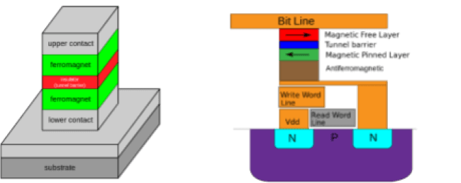
Credit: Wikipedia
Importance of Spin Transfer Torque
If a memory device utilises MTJs, then it is required to be able to change the magnetic polarisation of the free layer. While external current can be used to provide a magnetic field, it is not efficient and leads to both large power consumption as well as increased write times. To get around this, electron spin can be exploited to significantly reduce both the needed current while reducing the access time. An electric current is often unpolarised having around 50% spin-up and 50% spin-down, but if this current is passed through a sizeable magnetic layer, then the resulting current will have a spin bias (i.e. not a 50/50 distribution of spin). When this current is then passed through a free-layer, then that free-layers magnetic polarisation will line up with the polarised current.
Reliable 1X nm STT MRAM
A team of researches from Tohoku University lead by Testuo Endoh have announced the development of an MTJ in the 1X nm size. The device, which utilises magnetoresistivity and spin-transfer torque has a write time of 10ns, has an endurance of up to 1011, and can hold data for over ten years. Creating the device involves multiple layers, including numerous MgO barriers which separate the magneto layers. The benefits of this development are realised when compared to modern memory requirements. When choosing a memory technology for any application, it is often needed that the memory can handle a specified number of write cycles. For example, SSDs that store files are only expected to be occasionally written thus utilise FLASH technology while RAM is expected to be written millions of times a second thus utilising either DRAM or SRAM technology. Another area that has to be considered is power consumption; desktop PCs have an unlimited supply of power, but their battery size limits mobile devices. Therefore, a mobile device will use a smaller lower frequency memory that offers better power performance when compared to high-speed DRAM found in large computers.
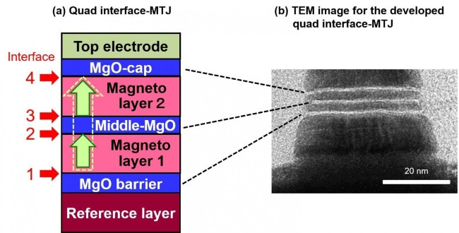
Credit: Tohuku University
The development of the 1X nm STT MRAM by the research team has produced a device that is faster, and more efficient than other technologies, making MRAM devices more desirable in memory applications. While MRAM devices do exist, their use is not widespread and is limited to niche applications. But the implications of MRAM are far more significant than most memory technologies as it could be the universal memory of the future
What is Universal Memory?
Depending on the requirement, multiple memory technologies exist. Hard disks are used to store large amounts of data for long periods while DRAM provides processors with high-speed memory for storage of running applications. The reason for this diversity in memory is that each memory technology has its advantages and disadvantages; thus, no one memory technology could be used for everything. FLASH is great for long term data storage but would quickly degrade if used as RAM while a hard drive is far too slow to use as RAM. If, however, a memory technology could work in all applications then it would be considered to be a universal memory solution; one that can be used in RAM, storage, and cache with no performance drop in any of the applications. This is something that MRAM may offer engineers if it can be shown to have an endurance cycle that on par with DRAM. Its high speed enables it to be used as RAM while its non-volatile behaviour allows for it to store information. But how would a universal memory system look to a designer? Would it have a single memory space for RAM and file storage? That is something only time will tell!
