Quantum dot of gold could be the transistor of tomorrow
| 11-06-2019 | By Rob Coppinger
A two-dimensional (2D) quantum dot of gold could be the transistor of tomorrow’s electronics but 2D microchips are too small to make with today’s lithographic technologies.
For decades, the law that describes how computers double their performance every 18 months, Moore’s law, has been proven correct as electronics have become smaller and more powerful. To continue that trend will require the manipulation of atoms to create components just a few nanometres in size. A transistor on this nanometre circuit could be a two-dimensional (2D), monolayer clump of gold atoms (monatomic), a unique 2D quantum dot, which is located on top of a graphene or nanotube substrate. The gold dot replicates a transistor’s function, stopping a current, acting as a switch, transferring a single electron at a time. The challenge is in fabricating such electronics because 2D quantum dots are so sensitive, even a single extra atom may change their performance.
“We know that current lithographic [processes], even including the best electron beam lithography, it is hard to go down to single digit [nanometre] accuracy, down below 10nm,” said Michigan Technological University physics professor, Yoke Khin Yap. “We are talking about a quantum dot which is a few nanometres [in size].”
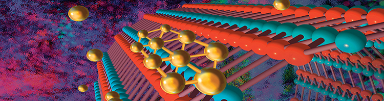
Two-dimensional quantum dots of gold are promising for quantum computing and future electronics. Credit: Michigan Technological University
Proof of concept
To build a proof of concept 2D quantum dot device, Yap thinks, “real primitive techniques,” might be needed and he is referring to the use of adhesive tape. The adhesive on the tape can be used to strip an atomic layer of material from one source and to add those atoms to another substrate. “Adhesive tape will require a lot of trial and error to find a way of getting a single layer,” he explained.
Graphene, a monolayer of graphite, has been proposed for 2D electronics but while it is very conductive, electrons flow very quickly, it cannot be used for a transistor; because the electrons will not stop. Transition Metal dichalcogenides are the focus for the transistor, but many candidates have low conductivity, low electron mobility. Yap admits that his team does not know how fast electrons flow through 2D gold or other 2D metals, “but based on the physics behind it…there will be uniform flow, so you can expect uniform and potentially high mobility.”
In his work, Yap used boron nitride nanotubes for the substrate. Using a scanning transmission electron microscope, gold atoms were monitored as they interacted with the surface of boron nitride nanotubes. The gold atoms, initially in mist form, settled on the nanotube hexagon honeycombs after gliding along the surface. Eventually gold atoms begin to clump, preferring to deposit with other gold atoms, creating the monatomic quantum dot. For the next step of finding that commercially viable manufacturing process, “we might need some beyond the box ideas,” Yap added.
He expects the two-dimensional electronics to have applications in optical and quantum computing and related areas such as photovoltaics and biosensing. The work was carried out in collaboration with another Michigan Tech physics professor, Ravindra Pandey, whose team contributed the theoretical model, and researchers at the Oak Ridge National Laboratory’s Center for Nanophase Materials Sciences.