Hobbyist Semiconductor Dopant Using Spin-On Glass
Insights | 03-07-2025 | By Robin Mitchell
Key Takeaways:
- A hobbyist-developed spin-on glass dopant offers a cost-effective alternative to commercial semiconductor doping techniques.
- This method uses safer, accessible chemicals like boric acid and phosphoric acid, eliminating the need for hazardous industrial gases.
- The DIY doping process employs thermal diffusion and TEOS-based sol-gel chemistry to achieve precise, repeatable results.
- With implications for education, research, and legacy chip production, this innovation helps democratise semiconductor fabrication.
While the spotlight often falls on the latest chip release or a headline-grabbing AI tool, the real story of technological progress often plays out quietly—behind lab benches, on community forums, and in makeshift home labs. Over time, innovation doesn’t just race ahead; it leaves behind accessible tools and techniques that once seemed out of reach.
So what happens when yesterday’s cutting-edge tech becomes today’s weekend project? How does engineering evolve when the tools of industry trickle down into the hands of hobbyists, students, and solo builders? And what can we learn from the hidden cycle of innovation that empowers not just corporations, but individuals?
How Technology Advances Through the Years
Every year, without fail, we're introduced to another wave of "the next big thing." Whether it's a new microcontroller, an overhyped AI framework, or some miracle material pulled out of a university lab, the pace of technological advancement doesn't let up. For those of us in engineering, it's equal parts exhilarating and exhausting.
With every leap forward, yesterday's breakthroughs quietly shuffle toward the exit. Hardware that was once cutting-edge gets declared obsolete, and software frameworks that ruled the previous decade find themselves unsupported, deprecated, or completely rewritten by some hipster startup.
Now, in many cases, the old stuff can be maintained. Anyone who's worked in industrial automation knows full well that there are still 20-year-old PLCs controlling equipment because "it still works." But even those eventually give out—and more importantly, the knowledge and components needed to keep them running dry up.
From Obsolescence to Opportunity: How Old Tech Becomes Accessible
However, as new tech replaces the old, one of the most beautiful patterns in engineering history emerges: as new tech rises, old tech democratises. The production methods, knowledge, and tooling once locked behind million-dollar R&D budgets become accessible to regular folks. What was once bleeding-edge becomes breadboard-ready.
Take semiconductors. In the early days, building a single transistor required a cleanroom, a PhD, and the GDP of a small country. Now? We've got YouTubers building working transistors with little more than a toaster oven, a glass slide, and a good microscope. Is it practical? No. Is it awesome? Absolutely.
Same story with computing. The behemoth machines IBM used to lease out for a fortune now fit in your palm and run on a few bucks' worth of silicon. In fact, entire retro-computers that once filled server rooms can now be built by hobbyists over a weekend for under $100. That's not regression—it's empowerment.
What many see as obsolescence is actually just a natural shift of capability from industry to the individual. Yesterday's proprietary manufacturing processes have become today's DIY projects. As innovation moves forward, it quietly leaves behind a trail of tools, techniques, and technologies that become open to everyone.
And that's the hidden genius of technological progress—it doesn't just move us forward. It also lowers the bar of entry behind it, allowing the next generation of engineers, makers, and tinkerers to stand on the shoulders of what once seemed unreachable.
So while the latest chip release might grab headlines, don't ignore the quiet power of yesterday's tech becoming today's playground. In the right hands, that's where real innovation starts.
Semiconductor Doping Made Affordable for Hobbyists
Researchers and engineers have long understood the importance of semiconductor doping in the field of electronics. The ability to control the electrical conductivity of materials has been crucial in the development of numerous electronic components, including transistors, diodes, and integrated circuits. However, the high cost of semiconductor dopants has traditionally been a barrier to entry for hobbyists and makers looking to experiment with semiconductor fabrication.
What makes this development particularly notable is that traditional dopants used in industry—such as phosphine and diborane—are not just expensive, but also hazardous to handle. ProjectsInFlight circumvented this by experimenting with safer, readily available compounds like boric acid and phosphoric acid, reducing both cost and health risk. This careful choice of materials aligns with the practical constraints faced by most hobbyists, especially those working from home setups without access to fume hoods or advanced lab infrastructure.
Safer Alternatives to Industrial Dopants for Home Fabrication
Recently, a maker by the name of ProjectsInFlight has successfully developed a homemade semiconductor dopant, marking a significant achievement in the field of affordable semiconductor fabrication. In a recent blog post, ProjectsInFlight outlined the steps taken to create the dopant, which utilises thermal diffusion doping to introduce phosphorus or boron atoms into silicon wafers.
This detailed video by ProjectsInFlight provides a step-by-step breakdown of the doping process, including the practical considerations and challenges involved. It serves as a valuable companion to the written guide, offering visual clarity for makers looking to replicate the method safely and effectively.
In one experiment, a donor wafer was coated with a phosphorus source and placed adjacent to a clean wafer inside a furnace. At high temperatures, phosphorus vapour diffused into the clean wafer. Although this approach achieved only light doping, it demonstrated a safe, effective method that does not rely on direct contact or toxic gases—important for non-professional environments.
Applying Thermal Diffusion Doping in Hobbyist Environments
Thermal diffusion doping is a process that involves placing a source of doping atoms on top of a silicon wafer and heating it to a high temperature. The resulting diffusion of doping atoms into the silicon crystal structure allows for precise control over the electrical conductivity of the material. While this process has been widely used in commercial semiconductor fabrication, the high cost of specialised equipment and chemicals has made it inaccessible to hobbyists.
Instead of relying on traditional solid sources or gas-phase dopants, ProjectsInFlight introduced a spin-on method using a homemade liquid solution. The key innovation lies in using a silicate precursor that converts into a doped glassy layer during high-temperature processing. This method eliminates the need for high-vacuum systems or gas handling, both of which pose serious barriers for amateur fabrication.
ProjectsInFlight's homemade dopant utilises a spin-on glass doping technique, which involves applying a thin layer of precursor chemicals to the silicon wafer. Upon heating, the precursor chemicals decompose to form a protective glass layer that contains the doping atoms. As the wafer is heated, the doping atoms diffuse out of the glass layer and into the silicon crystal structure, allowing for precise control over the doping levels.
Notably, the final recipe for a phosphorus dopant included tetraethyl orthosilicate (TEOS), ethanol, water, and phosphoric acid. These ingredients were carefully balanced to form a stable sol-gel mixture, which could be spin-coated and later heat-treated to form a uniform glass film. ProjectsInFlight reported that the processed wafers showed resistivity consistent with heavily doped silicon, supporting the effectiveness of this low-cost approach.
Formulating a Reliable, Cost-Effective Spin-On Phosphorus Dopant
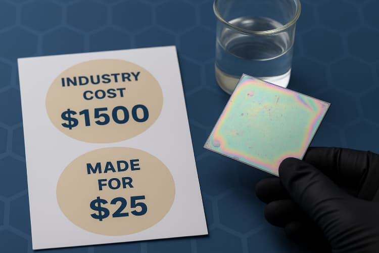
The development of this homemade dopant is a significant achievement for the maker community, as it provides hobbyists with a cost-effective solution for semiconductor fabrication. The dopant is approximately two orders of magnitude cheaper compared to commercial products, making it an attractive option for those looking to experiment with semiconductor design and fabrication.
Aside from reducing cost, the project emphasised safety and accessibility. Unlike conventional spin-on dopants sold to industry—which require freezer storage and have limited shelf lives—this DIY solution was designed to be more robust. The use of TEOS-based chemistry also leverages known sol-gel principles used in university labs, further reinforcing the credibility and educational value of the process.
While the homemade dopant is still in its early stages of development, it has already shown promising results. In a recent experiment, ProjectsInFlight was able to successfully dope silicon wafers, demonstrating the effectiveness of the dopant. The ability to control doping levels with high precision also allows for the creation of complex semiconductor structures, which could be used in a wide range of applications, including transistors and integrated circuits.
Early Success and Educational Potential of DIY Doping Techniques
The development of this affordable semiconductor dopant also has implications for the field of education and research. The high cost of commercial dopants has often been a barrier to entry in semiconductor fabrication courses and research projects, limiting the number of students and researchers who can participate. The availability of a cost-effective dopant solution could help to democratise access to semiconductor fabrication, allowing more individuals to explore the field of semiconductor design and fabrication.
For educational institutions operating on tight budgets, this method could serve as a hands-on introduction to solid-state physics, materials science, and microfabrication. ProjectsInFlight even demonstrated hot-probe testing to verify doping type—N-type and P-type—highlighting how such basic experiments can validate real-world semiconductor behaviour without requiring commercial-grade metrology tools.
With more refinement, there is potential to extend this methodology toward other dopants or substrate types. While commercial fabs optimise for scale, hobbyist-led efforts like this prioritise simplicity, safety, and cost-efficiency—principles that resonate with educational labs, small-scale prototyping, and niche component reproduction.
Could This New Dopant Be the Catalyst for Homegrown Semiconductors?
This new homemade semiconductor dopant isn't going to knock Intel or TSMC off their pedestals. It won't power the next iPhone, and it won't compete with the bleeding-edge 2nm nodes. But that's not the point—and it never was.
What it will do is far more exciting for those of us who care about access, innovation, and bringing control back to the hands of individuals. The development of affordable doping methods, like the one recently demonstrated by ProjectsInFlight, could very well be the start of something much bigger: the democratisation of semiconductor fabrication.
For too long, semiconductors have existed behind billion-dollar walls. Clean rooms, multi-step lithography, exotic chemicals—it's an exclusive club. But the discovery that a spin-on glass dopant can be made cheaply and used effectively cracks open that door. Suddenly, it's not unthinkable for an electronics enthusiast to experiment with basic transistor fabrication in their garage or lab.
Now, these DIY chips aren't going to end up in mission-critical avionics systems. But they might end up in the hands of a curious high schooler who stumbles into a lifelong passion for semiconductor physics. Or a university student who builds a working bipolar junction transistor from scratch for their thesis. Or a garage entrepreneur who finds a way to remanufacture long-obsolete chips for legacy systems—industries that Big Silicon has long abandoned.
This isn't fantasy—it's precedent. We've seen this same story play out before. Once upon a time, computing was locked in the hands of government labs and corporations. Then the homebrew computing movement kicked off. The result? Apple, Microsoft, and the entire modern tech economy. That started with hobbyists, not MBAs.
More practically, this kind of accessible doping technique opens up real-world possibilities for specialised, small-scale foundries. As commercial fabs continue to focus exclusively on the newest, fastest, smallest transistors, the world is left with a growing problem: older chips—think 7400 logic ICs, early microcontrollers, or specialty analog parts—are vanishing. But if small teams or independent makers can economically produce replacement parts, suddenly you're looking at a viable business model, without needing a nine-figure clean room.
And that's the real story here.
This homemade dopant isn't the endgame. It's a beginning. A humble, experimental tool that—like all great tools—opens new doors. I expect it will encourage a new generation to stop being passive consumers of tech and start becoming creators. Tinkerers. Builders. Engineers.
Personally? I'll be watching this space very closely. Not because it's going to flip the industry overnight, but because it's a spark. And history shows us that sometimes, it only takes one to light the fire.
