Fix Point Defects in Semiconductors at 200°C with MoS₂
Insights | 17-06-2025 | By Robin Mitchell
Key Takeaways:
- A new low-temperature technique using PFBT has been developed to repair sulphur vacancies in molybdenum disulfide (MoS₂), a key material for next-generation semiconductors.
- The method restores the atomic structure of MoS₂ at just 200°C, making it compatible with industry-standard BEOL processes that demand low thermal budgets.
- Transistor devices fabricated with repaired MoS₂ showed a 2.5x improvement in charge mobility and a 40% reduction in subthreshold swing, supporting high-speed, energy-efficient operation.
- This innovation may help reduce chip production costs, increase wafer yields, and enable more compact and reliable semiconductor designs.
As microchips continue to power every aspect of our digital world, the pressure to shrink transistor sizes has never been greater. Yet with this miniaturisation comes a host of complex challenges—chief among them, the emergence of atomic-scale defects that compromise performance and reliability. A recent breakthrough from researchers at UNIST and POSTECH tackles this issue head-on with a novel technique to repair defects in molybdenum disulfide (MoS₂), a promising material for next-generation semiconductors.
What obstacles do miniaturised transistors face, how does this new defect repair method work, and could it revolutionise the future of semiconductor manufacturing?
Shrinking Transistors – The Challenge Behind Modern Microchips
Microchips, alongside the transistor itself, stand as one of the most important technological breakthroughs of the 20th century. Their widespread deployment has enabled the entirety of modern digital life, from smartphones and cloud computing to advanced robotics and connected infrastructure. The rapid pace of their development is not just impressive, it's foundational to the continued evolution of global technology.
The Shrinking Transistor: A Catalyst for Modern Innovation
One of the key driving forces behind this progress has been the relentless push to shrink transistor sizes. Smaller transistors allow more to be packed into a given area, enabling faster, more efficient processors with lower power consumption. This phenomenon, famously described by Moore's Law, has held for decades thanks to cutting-edge manufacturing and deep innovation. However, as with all engineering progress, these advances come with significant challenges.
At nanoscale dimensions, transistor behaviour becomes far more complex. Quantum effects, such as electron tunnelling, start to interfere with standard device operation. Traditional fabrication techniques like photolithography face physical limits when defining features smaller than the wavelength of light used to pattern them. But among the more insidious challenges is the issue of point defects.
Atomic-Scale Defects: The Hidden Barrier to Reliable Performance
Even with ultra-pure silicon wafers and highly controlled fabrication environments, atomic-level imperfections are inevitable. A single misplaced atom or impurity at the wrong location can disrupt the function of a transistor. At these scales, there is no margin for error. These point defects can reduce performance, lead to unpredictable behaviour, and in worst cases, cause device failure.
Unlike traditional faults that can be debugged or repaired at the circuit level, point defects are essentially baked into the material. Once a chip is fabricated, these defects are nearly impossible to detect or correct, leading to lower manufacturing yields, increased costs, and greater variability in device performance.
While industry continues to innovate around these problems, through advanced error correction, redundancy, and novel materials, there's no denying that we're approaching the physical limits of what silicon-based technology can deliver. This is why continued research, private sector leadership, and engineering innovation remain critical. The future of electronics depends not just on making things smaller but smarter at every level of design and production.
Researchers Develop Defect Removal Technique for Next-Generation Semiconductors
In a new discovery that could pave the way for the development of faster, low-power semiconductors, a team from the Ulsan National Institute for Science and Technology (UNIST) and the Pohang University of Science and Technology (POSTECH) has successfully developed a defect removal technique for molybdenum disulfide (MoS₂). This new technology, which operates at temperatures as low as 200°C, represents an essential advance toward the commercial use of MoS₂ as a next-generation semiconductor material.
In particular, the technique’s compatibility with the 200°C thermal threshold significantly enhances its potential for integration within modern semiconductor manufacturing workflows, which are tightly constrained by thermal budgets. This detail not only underlines its industrial viability but also aligns with BEOL requirements that dominate silicon device assembly pipelines, where excessive heat can critically impair layer integrity.
Enabling Low-Temperature Integration of Advanced Materials
MoS₂ is a promising candidate for the development of next-generation semiconductors and has the potential to increase chip density and minimise leakage current. This could ultimately lead to the creation of heat-free, low-power semiconductors that are highly sought after by the industry. However, the integration of MoS₂ into actual chips is presently a challenging task due to defects that occur during the deposition process.
These deposition-related defects—primarily sulphur vacancies—are known to compromise charge transport efficiency by disrupting the material’s atomic lattice. Such inconsistencies directly affect device stability and degrade overall performance, particularly in high-density logic architectures where uniformity is non-negotiable.
Removing these defects is crucial for the commercialisation of MoS₂, as the deposition of MoS₂ on silicon devices must be carried out without damaging existing silicon components. Since high temperatures can be detrimental to silicon components, it is essential to develop a defect removal technique that operates at low temperatures.
The low-temperature threshold is especially critical for BEOL integration, as the industry standard dictates process temperatures remain below 350°C. The ability to repair MoS₂ at 200°C, as demonstrated in this study, therefore opens new pathways for incorporating 2D materials without compromising existing device structures or interconnects.
Chemical Repair of MoS₂ Defects at Industry-Compatible Temperatures
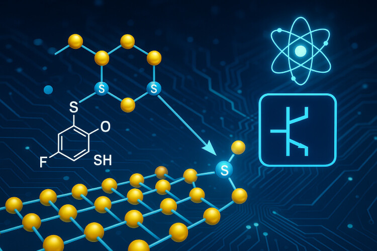
In their study, the researchers used pentafluorobenzene thiol (PFBT), a compound containing a hexagonal benzene ring with both a thiol (-SH) and a fluoro (-F) functional group. The sulfur atom in the thiol group directly fills the sulfur vacancies in molybdenum disulfide (MoS₂), while the fluorine atoms facilitate the removal of the remaining non-sulfur portion of the molecule following the reaction. The viability of this mechanism was supported by molecular dynamics simulations, and X-ray spectroscopy confirmed that the sulfur vacancies in MoS₂ were effectively repaired at temperatures as low as 200°C.
X-ray photoelectron spectroscopy (XPS) analysis was instrumental in confirming the successful passivation of sulphur vacancies. The data revealed a restored Mo:S atomic ratio approaching 1:1.98—close to the ideal 2:2 stoichiometry—underscoring the method’s precision in defect correction. This degree of atomic-level control supports robust electronic characteristics critical for scaling semiconductor applications.
The researchers also fabricated transistor devices using the repaired MoS₂ and found that the charge mobility of the devices was improved by 2.5 times compared to devices with defects in the MoS₂. Faster charge movement correlates to quicker operational speeds, and the sub-threshold swing value, a critical metric for power consumption, was reduced by approximately 40%. The results of the study confirm the effectiveness of the defect removal technique and highlight the potential of MoS₂ as a next-generation semiconductor material.
Additionally, devices built using the repaired MoS₂ demonstrated significant reductions in subthreshold swing, a key parameter in low-power operation. With an approximate 40% improvement, this optimisation aligns closely with emerging energy efficiency standards and enhances the feasibility of MoS₂-based FETs in portable electronics and edge computing devices.
Performance Gains and Commercial Integration Potential
The defect removal technique developed by the researchers is also compatible with existing silicon semiconductor back-end-of-line (BEOL), which is a process that connects previously deposited components on an integrated circuit. The BEOL process must be carried out at temperatures below 350°C to avoid damaging the devices, and the researchers' technique can be used at temperatures of 200°C or lower, making it a viable option for commercialisation.
The method’s alignment with industry constraints—particularly its ability to coexist with silicon fabrication ecosystems—positions it as a bridge between established semiconductor platforms and next-generation 2D materials. This interoperability will be essential for practical adoption in heterogeneous integration frameworks, where modular and scalable manufacturing is the end goal.
Could This Development Change the Future of Microchips?
While the current research is specific to MoS₂, the implications of such a technique being adapted for silicon-based devices are considerable. Silicon remains the cornerstone of the semiconductor industry, and the ability to fix point defects in silicon wafers would unlock unprecedented possibilities. Firstly, if engineers could reliably repair defects, the need for redundant circuitry within devices would be considerably reduced. Currently, to mitigate the impact of manufacturing defects, chips are often designed with redundant circuits, which take up valuable space. By eliminating the necessity for these redundancies, more chip area could be dedicated to functional circuits, enhancing the overall computational power and efficiency of the device.
Additionally, the ability to repair point defects could dramatically increase the yield of semiconductor wafers. Presently, a large portion of wafers are being discarded due to defects, which are driving up production costs. By pushing yields closer to 100%, the cost of chips could be reduced, making advanced technology more accessible. This cost reduction could have a ripple effect across various industries, from consumer electronics to automotive and aerospace, where high-performance semiconductors are crucial.
Boosting Yield and Enabling Compact, Energy-Efficient Designs
In addition to cost savings, the elimination of redundant circuits would allow for the production of smaller, more compact chips. Many chips today are composed of multiple identical units, with some units enabled and others disabled to compensate for defects. By ensuring that each unit is defect-free, engineers could design more streamlined chips, conserving space and potentially reducing power consumption. This is particularly vital in the era of mobile devices and Internet of Things (IoT) technology, where space and energy efficiency are paramount.
Finally, repairing point defects could help each semiconductor device reach its maximum performance capabilities. Defects often lead to variability in device performance, with some chips operating slower or consuming more power than others. By addressing these imperfections, engineers could ensure that every chip performs at its peak, delivering consistent and reliable performance across all applications. This uniformity is especially critical in high-reliability fields such as medical electronics and aerospace, where even minor performance deviations can have serious consequences.
The research on MoS₂ defect repair is a clear indication of the creative spirit driving the semiconductor industry forward. While challenges remain in adapting these techniques to silicon and other materials, the potential benefits are too compelling to ignore.
