Canon vs. ASML: New Advances in Lithography
Insights | 20-11-2023 | By Robin Mitchell
The recent reveal of Canon’s latest lithographic offerings showed that competitors such as ASML could have their work cut out for them, and many wondered if the technology could get around existing trade restrictions on China. What challenges does China face in terms of lithography, what did Canon develop, and could this new technology be sold to Chinese interests?

What challenges does China face in terms of lithography?
To say that China has faced immense challenges with regard to its semiconductor industry over the past few years is an understatement. As China attempts to become a superpower in the field of electronics, its actions against its own citizens, its neighbours, and other countries around the world have seen the West push back against its developments through the use of trade restrictions.
One notable restriction that the West has imposed is the banning of high-tech equipment used to produce nanometre node semiconductors, such as lithographic systems manufactured by ASML. While it is still possible to produce high-end semiconductors with older imaging systems, the results are often difficult to repeat and impose a significantly higher price on semiconductors due to the lower yields.
This was demonstrated in the latest Huawei smartphone, the Mate 60, which included 7nm devices that many thought China was unable to produce and yet had done so with the help of older ASML lithographic systems. Of course, 7nm is still a number of years behind what Western foundries are able to produce, with some now turning out 3nm and others practising with 2nm features.
To make matters worse for Chinese manufacturers, not only is China barred from accessing advanced lithographic systems, but it is also barred from ordering high-tech parts as well as placing custom orders from foundries such as TSMC. This was demonstrated when the Mate 60 phone was found to contain SK Hynix memory chips, something which it should have never had.
Considering that China was arguably at the forefront of AI technologies at the start of the decade, these actions by the West have undoubtedly pushed back China’s ability to develop such technologies and may even have fallen behind the West now that computing systems used by the West are able to take advantage of the latest nodes.
Canon’s lithographic offerings threaten ASML
The intricate world of semiconductor chips surpasses common expectations. It's astonishing to learn that the total circuit length in a chip, just centimeters in size, exceeds the length of a marathon. This fact alone underscores the remarkable complexity and miniaturization inherent in modern semiconductor technology.
Across the semiconductor industry, ASML has an absolute monopoly on lithographic systems, especially those used in next-generation nodes. This monopoly has both advantages and disadvantages, with one example of an advantage being the ability to prevent hostile nations from developing chips and an example of a disadvantage being the issue with pricing and control.
However, a recent development by Canon could put ASML’s monopoly at risk and even has the potential to provide China with an alternative lithographic technology in the future. The new technology, called nano-imprinting lithography, allows for the creation of nodes down to 5nm, something which currently requires extreme UV systems to do.
Canon's innovative approach in semiconductor manufacturing also includes leveraging its ink ejection technology, originally developed for inkjet printers. This cross-industry application is used for precise resist dispensing in NIL, exemplifying Canon's ability to creatively adapt existing technologies for groundbreaking purposes.
Furthermore, it was also claimed by Canon that ongoing improvements in the technology could even see 2nm devices produced. But the new technology isn’t just able to do what current ASML systems are capable of. Canon has also claimed that it will be able to do so at a lower cost, thereby potentially undercutting ASML.
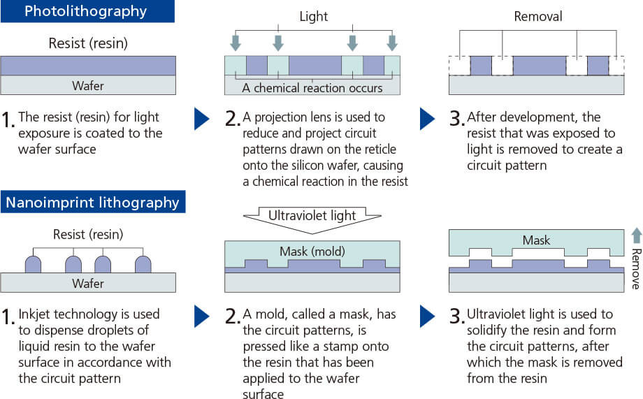
Without going into too much detail, the new technology developed by Canon applies a circuit pattern to a resist stamp, which then gets pressed into a silicon wafer instead of applying a layer of resist to a wafer and then etching a design onto it. The new technology eliminates the need for the circuit pattern projection step, something which requires extremely advanced mirrors and lenses.
According to Canon, the new technology could see a price figure that is one less digit than that currently offered by ASML (thus, approximately a ten times saving).
A New Era in Lithography: The Simplicity of Canon's Nanoimprint Method
While photolithography has been a cornerstone in the evolution of semiconductor chips, driving down costs and enabling the miniaturization of technology, it has reached a point where further miniaturization has become a complex challenge. This pursuit of smaller circuitry has led to the development of increasingly larger and more expensive lithography systems, pushing the boundaries of technological and economic feasibility.
In this context, Canon's introduction of nanoimprint lithography (NIL) marks a significant shift. Unlike the intricate and costly process of photolithography, NIL adopts a more straightforward approach. It involves physically pressing patterns from a mask directly onto the resin. This method is not just simpler but also more cost-effective, potentially revolutionising the economics of semiconductor manufacturing.
Moreover, the precision offered by this stamp-like approach in NIL results in extremely sharp and accurate circuit patterns. This level of precision is not just about achieving smaller sizes; it also plays a crucial role in enhancing the quality of the chips. Sharper patterns mean lower defect rates, which is a critical factor in the semiconductor industry where reliability and efficiency are paramount. Therefore, Canon's NIL technology doesn't just promise cost savings; it also contributes to the production of higher quality, more reliable semiconductor chips.
Breaking Down Canon's Nano-Imprint Lithography: A Technological Leap
Delving deeper into Canon's groundbreaking NIL technology, it's evident that this isn't just a marginal improvement but a paradigm shift in semiconductor fabrication. Canon's approach, which involves a resist stamp directly imprinting patterns onto silicon wafers, bypasses the limitations of traditional photolithography. This method, known as nanoimprint lithography, is not only more cost-effective but also significantly increases the precision of semiconductor patterning, potentially enabling the production of circuits as small as 2nm.
A critical aspect of Canon's NIL technology is its extraordinary precision. The company has developed a method to overlay circuit patterns with accuracy finer than one nanometer. This level of precision is crucial in the stacking of countless layers of circuit patterns, a common practice in modern semiconductor chips.
Canon's innovation in NIL technology is underpinned by several key advancements. These include a unique resist material that improves the imprinting process and a sophisticated alignment system that ensures nanometer-level precision. This technology, while reducing costs, does not compromise on the quality or complexity of the semiconductor designs it can produce, making it a formidable competitor in the lithography market.
Could the new technology be the solution to China’s challenges?
While the new technology is certainly not the same as ASML, it would still be covered by Japan’s current trade restrictions with China. As such, the new technology would still be unavailable to China and, therefore, keep China away from cutting-edge semiconductors.
However, there is a silver lining for China in this current situation; UV projection is not the only way to make a semiconductor. If the method developed by Canon can be made economical, then it proves that there is more than one way to produce semiconductor devices, and this could be all the drive that China needs to develop its own solution.
For example, it may turn out that China ends up developing an ion-beam etching device that is able to produce nanometre-sized features rapidly. By making China desperate for technology, there is plenty of incentive and money to go around inside China to make large leaps and bounds in the field of semiconductors. In fact, this has already been seen with China’s advances in homegrown semiconductors and work on RISC-V devices.
The implications of Canon's NIL technology extend beyond just an alternative to ASML's offerings. It represents a significant leap in semiconductor manufacturing, potentially reshaping global semiconductor supply chains. If Canon's technology becomes widely adopted, it could alter the competitive landscape, offering countries like China new avenues to circumvent current technological limitations imposed by trade restrictions.
If the West isn’t careful, it’s possible that China will be forced into desperation for semiconductors, and this could not only see China rapidly accelerate its semiconductor capabilities but even potentially outshine the West, giving it a technological edge.
