MIT Engineers Develop Atomically Thin Transistors on Silicon Chips
Insights | 09-05-2023 | By Robin Mitchell
Recently, researchers from MIT demonstrated a new technology that allows atomically thin transistors to be fabricated on top of pre-existing silicon dies, paving the way for future devices with multiple transistor layers.
However, as the size of transistors continues to shrink, semiconductor manufacturers face increasing difficulties preventing them from creating smaller devices. One such challenge is that the space between gates and channels has become so small that electrons are able to jump the barrier via electron tunnelling, reducing the amplification capabilities of transistors and increasing leakage current.
Another challenge faced is that as transistors become smaller, point defects in the semiconductor lattice are more likely to cause a chip to fail, leading to lower yields per wafer and increasing the cost of each working chip. One solution around these issues is to create 3D devices with additional active layers to increase the overall transistor count. However, this presents its own set of challenges, such as growing transistors at high temperatures that can damage pre-existing transistor structures, as well as the difficulty of fusing two chips together.
Fortunately, researchers from MIT recently developed a new method for growing transistors on top of silicon chips using 2D metal dichalcogenide materials that can be grown at lower temperatures, reducing the potential for damage to pre-existing structures. This breakthrough could potentially pave the way for highly advanced chips of the future and flexible electronics. What challenges do 3D chips present, what did the researchers develop, and how could it be useful for future applications?
What challenges do 3D chips present?
As the world enters a new era of technology with AI and augmented systems rapidly taking over, the importance of powerful processors continues to be a dominating factor in the semiconductor industry. While the development of cloud systems allows for local devices to utilise low-energy processors that have limited performance capabilities, the need for high-performance capabilities from the server side has never been more important. For example, large AI language models such as ChatGPT require extensive amounts of processing capabilities, high data bandwidth, and countless amounts of high-speed storage, while connected clients only need to have the ability to form an internet connection, provide a prompt, and read the result.
However, as the size of transistors continues to shrink, semiconductor manufacturers face increasing difficulties preventing them from creating smaller devices. One such challenge is that the space between gates and channels has become so small that electrons are able to jump the barrier via electron tunnelling, and this not only reduces the amplification capabilities of transistors but also increases leakage current. While the new method of growing atomically thin transistors on top of pre-existing silicon dies shows promise for creating highly advanced chips in the future, there are still potential limitations and roadblocks that need to be addressed. For instance, the method may require further refinement to improve the uniformity of the grown layers, which could impact the overall performance of the transistors. Additionally, it is still unclear how easy it will be to integrate these transistors into the underlying semiconductor wafer and turn them into functional circuits.
Another challenge faced is that as transistors become smaller, point defects in the semiconductor lattice are more likely to cause a chip to fail. As such, designs that have billions of transistors will typically have a lower yield per wafer, and this increases the cost of each working chip.
One solution around this issue is to try and create 3D devices that focus on adding additional active layers to increase the overall transistor count. However, this is plagued with its own range of problems, so much so that modern 3D devices are generally limited to NAND flash. One such issue is that the high temperatures needed to grow transistors will quickly damage any pre-existing transistor structure already fabricated.
It is also possible to stack chips into 3D structures, but while this can be used to increase transistor count, it rapidly increases the vertical height of a device, and trying to fuse two chips together can be extremely difficult. Instead, modern chiplet designs will utilise multiple chips attached to a common substrate and small wires are used to connect the chips together.
MIT researchers grow transistors on top of chip
Recognising the challenges faced with 3D chips and the increasingly complex nature of modern applications, researchers from MIT recently published their findings on a new method for growing transistors on top of silicon chips.
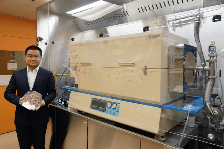
The new method takes advantage of 2D metal dichalcogenide materials that can be grown at temperatures significantly lower than the 400˚C mark (which sees degradation in silicon transistors). The two-chambered furnace used in this method allows for the growth of 2D metal dichalcogenide materials at lower temperatures than the standard method. In one chamber, the furnace is kept hot and used to decompose the molybdenum. The vapourised molybdenum then travels to the cooler chamber, where it is combined with sulphur to create the semiconductor material. This combination settles on the surface of the wafer, growing an atomically thin layer of semiconductor. The chosen material, molybdenum sulphide, requires temperatures exceeding 500˚C to manufacture, but the researchers were able to circumvent this issue with the use of a unique two-chambered furnace. One of these chambers is kept hot and is used to decompose the molybdenum, and once vapourised, it can travel to the cooler chamber, where it is combined with sulphur to create the semiconductor material. This combination then settles on the surface of the wafer, growing an atomically thin layer of semiconductor. Finally, to prevent the sulphur compounds from damaging the top layer of the semiconductor wafer (where aluminium is present), the researchers deposited a thin layer of boron nitride to isolate the grown molybdenum sulphide from the wafer. Overall, the new layer can be grown in a matter of hours with a great deal of uniformity over an 8-inch wafer.
The integration of 2D materials directly onto a silicon circuit using a new low-temperature growth and fabrication technology could potentially result in denser and more powerful chips.
The furnace consists of two chambers, one hot and one cold, connected by a small opening. In the hot chamber, the researchers decompose the molybdenum by heating it to high temperatures, which causes it to vaporize. The vaporized molybdenum then passes through the opening into the cold chamber, where it reacts with sulphur to form molybdenum sulphide, the semiconductor material. This combination then settles on the surface of the wafer, growing an atomically thin layer of semiconductor.
Finally, to prevent the sulphur compounds from damaging the top layer of the semiconductor wafer (where aluminium is present), the researchers deposited a thin layer to isolate the grown molybdenum sulphide from the wafer. The researchers deposited a thin layer of boron nitride to isolate the grown molybdenum sulphide from the wafer. The boron nitride layer is only a few atoms thick, but it effectively prevents the sulphur compounds from reacting with the aluminium layer on the wafer, which could cause damage to the device. Overall, the new layer can be grown in a matter of hours with a great deal of uniformity over an 8-inch wafer. Looking forward, the researchers hope that these layers can be turned into functional transistors and that additional layers of these transistors can be stacked.
The paper appears today in Nature Nanotechnology, a peer-reviewed scientific journal, after undergoing a rigorous evaluation process by experts in the field. The publication of this research in Nature Nanotechnology is significant because it represents a major breakthrough in the development of atomically thin transistors and could have far-reaching implications for the field of nanotechnology. By allowing multiple layers of transistors to be stacked on top of each other, this technology could pave the way for highly advanced chips that are more powerful, energy-efficient, and versatile than current designs. This could enable the development of new applications and technologies, such as highly complex AI systems, flexible electronics, and smart sensors. Additionally, the development of this technology could help to overcome the limitations of current semiconductor technology and drive further innovation in the field. This information could be inserted after the paragraph discussing the potential benefits of the new technology.
How could such technologies help with future designs?
Undoubtedly one of the biggest benefits that the research could provide is the ability to quickly increase transistor densities on chips. By creating 3D devices with multiple active layers, it would be possible to increase the overall transistor count, allowing for more complex and powerful devices. While the base layer can utilise standard silicon technologies for the most crucial circuit components, the additional layers could be used for static RAM, peripherals, and even low-speed neural net circuits. Such layers would also allow more space on the underlying chip to be dedicated to high-speed data processing, further increasing the capabilities of the device.
At the same time, the researchers also noted that the ability to grow large uniform layers of atomically thin semiconductors could also be used in a variety of smart devices, such as smartphones and wearables. This could allow for more powerful and energy-efficient processors that could handle complex tasks such as AI and image processing more efficiently. Additionally, atomically thin layers of semiconductor could be grown on fabrics to create sensors that can monitor vital signs, activity levels, and other health-related data in smart clothes and wearables. The technology could also be used in various smart devices, such as smart home appliances and security systems, by creating more energy-efficient and powerful processors with multiple layers of atomically thin transistors.
Overall, what the researchers have demonstrated is undoubtedly exciting and could pave the way for highly advanced chips of the future. For now, the researchers need to focus on turning the layer of semiconductors into functional transistors and circuits that can connect to the underlying semiconductor wafer.
