Sony 2-layer CMOS pixel sensors increase light sensitivity
| 01-03-2022 | By Robin Mitchell
Recently, Sony announced the development of its latest sensor technology that utilises stacked CMOS devices to improve light-gathering capabilities. What challenges do traditional CMOS sensors face, what did Sony develop, and how could the new technology help with camera technology?
What challenges do current CMOS sensors face?
Next to the development of colour film, capturing digital images directly has been one of the most outstanding achievements in imaging technology. Before digital cameras, the analogue film would need to be scanned into a computer to convert the image digitally. Even then, this would introduce problems such as resolution and colour quality. The introduction of digital cameras allowed for images to be stored electronically and allowed for in-camera processing such as white balancing, focusing saturation and hue adjustments, and noise removal.
For these reasons, digital cameras are the dominant type of camera technology in use. Of course, some enthusiasts do still use film, but such photography is generally for artistic or nostalgic reasons. However, there are some significant challenges that digital cameras continue to face.
One of these challenges is pixel size in CMOS cameras. For images to capture as much detail as possible, more pixels need to be obtained, which can be achieved by reducing the size of each pixel sensor. While this may increase the image resolution, it also reduces the amount of light received by each pixel, which can quickly introduce noise. This can be solved using a wider aperture, but wider apertures result in a shallow depth of field, creating images where only objects at a specific distance are in focus.
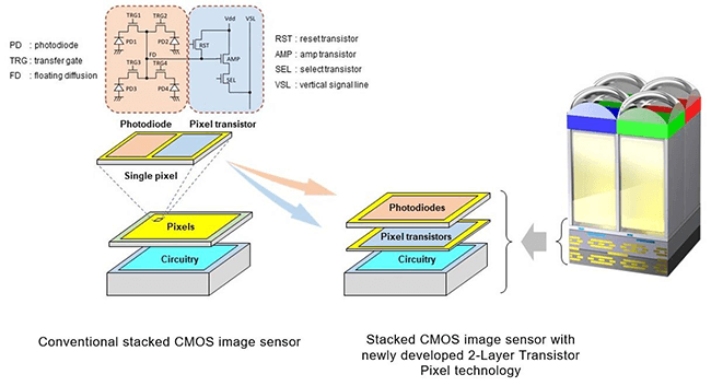
The second challenge relates to the first challenge: each pixel in a CMOS sensor requires multiple transistors for amplification and selection. The space used by additional support circuitry reduces the overall pixel count that is possible on a sensor, and this, in turn, reduces the resolution.
Sony develops a vertically stacked photosensor
These challenges of CMOS have recently been solved by Sony with their latest stacked CMOS photosensor design that places the active components for each pixel directly underneath each photodiode. Considering that the size of the control circuitry for each pixel is approximately the same as the size of the photodiode array (there are four diodes per pixel, one red, one blue, and two green), the effect is the doubling of pixel density.
However, instead of doubling the pixel density, each pixel can be enlarged by a factor of two, and this doubles the amount of light that each pixel receives. This increase in pixel area not only improves the sensor’s ability to work in low-light conditions but also reduces the amount of noise, allowing for improved images. Furthermore, the doubling of light intensity per pixel enables for higher f-stop apertures which increases the depth of field and thereby also increases the sharpness of images.
The shifting of the amplification transistors to their own layer below the photodiode layer has also allowed each transistor to be doubled in size, which further reduces the noise in the final image. The overall design has effectively three active layers that clearly demonstrates the benefit of multi-layers silicon technologies.
How could this new technology help with camera applications in the future?
The ability to create camera sensors that are more sensitive to light has major applications in the field of photography, whether it is astronomy, night vision, or monitoring. The low noise also makes it easier to identify objects and shapes in the dark, which could be crucial in future self-driving vehicles.
But the ability to gather twice the light also allows the sensor to be reduced in size by half for the same pixel count. This means that more compact cameras can be designed that could be fitted into applications where space is limited. For example, IoT security cameras could be given either better low-light capabilities or reduced in size (and therefore reduced energy consumption).
Fundamentally, what Sony has really demonstrated is the advantages of multi-layer semiconductors that have more than one active layer. This technique will not only improve camera sensors but can also help increase the performance of processors, increase memory density, and even improve power circuitry.
