Sam Zeloof’s 1000 transistor DIY chip
| 06-09-2021 | By Robin Mitchell
Sam Zeloof, an internet phenomenon in DIY ICs, has recently created a 1000 transistor chip from scratch. What equipment does he use, what did he recently achieve, and could the future see custom ICs?
Who is Sam Zeloof, and how was he able to produce DIC ICs at home?
Sam Zeloof is an American maker who was an undergraduate at CMU (as of 2018) and is most famous for developing DIY transistors at home. Another renowned maker, Jeri Ellsworth, demonstrated homemade transistors more than a decade ago, but Sam Zeloof has taken this a step further and produced custom DIY chips.
His first successful device was the Z1, a 6 transistor amplifier whose capabilities were demonstrated with a fully functional ring oscillator. Furthermore, the Z1is packaged in a DIP housing with gold microwires connecting the various pads on the chip to each pin.
Creating such a device is no small feat, and while the chip is homemade, the equipment used to make it is incredibly complex. For example, creating each layer on the silicon die requires physical vapour deposition, which was achieved using a high vacuum chamber and a plasma source. The setup to accomplish this involves using expensive turbopumps to create a near-hard vacuum while the plasma source is made from scratch using carefully machined parts, magnets, and complex engineering.
Another challenge faced by developing homemade ICs is the photoresist; while most of the chemicals used to create semiconductors can be readily found online and in stores, the photoresist is virtually inaccessible. Not only is the liquid costly (at $8000 per gallon), most suppliers will refuse to send out small quantities.
Adding gold microwires to the final chip required a specially donated wire bonding machine, and an electron microscope was used to help solve challenges faced when developing semiconductor devices. The devices produced by Sam Zeloof may be homemade, but they are far from being accessible to most.
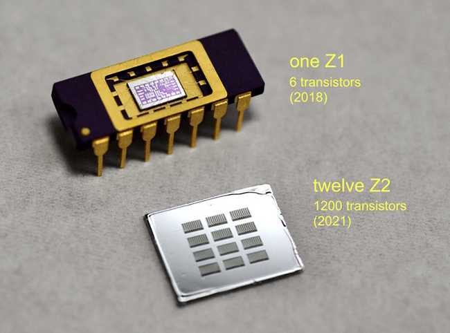
Z2 – The 1000 transistor mark
Recently, Sam Zeloof reported the successful creation of a chip with 1000 transistors putting its potential capabilities close to processors of the early 70s. The new device no longer uses aluminium as the gate electrode but instead polysilicon, creating transistors with far better performance. For feature size, the homemade Z2 1000 transistor chip uses a 10um gate process, and each prominent feature on the chip is a 10 x 10 array of transistors.
While the new chip has far more transistors than the previous designs, it comes with a few challenges. The first is that many transistors failed to operate as expected, which is low yield. Secondly, the device is purely N-MOS technology meaning that no complementary logic can be implemented, which would see far lower static power consumption.
Another challenge is that the 1000 transistor chip is a repeating pattern and not a single device meaning that each device produced is actually only 100 transistors. This may result from testing a small pattern, but it could also be related to the use of a projector with a fixed resolution. A fixed resolution from the project would mean that any single image projected onto the die would be limited in feature size and dimensions. Therefore, large designs have to be split up into sections and composited together.
Could the future see fully custom ICs?
The technology developed by Sam Zeloof is nothing compared to commercial semiconductor foundries, and it is almost certain that Sam will never achieve anything close to professional foundries. However, the ability to create custom transistors does have its advantages, and the development of the Z2 could be the start of homegrown ICs.
Specifically, businesses around individual chips could become a reality where engineers and makers alike wish to experiment with entirely custom silicon in their designs. This would enable designs to fully maximize their space while not integrating any components that are not absolutely needed. Furthermore, developing custom ICs could help with energy sensitive applications while simultaneously allowing for totally custom logic behaviour without the need for an FPGA or CPLD.
Looking at the future, a service that can create 100,000 transistor ICs with prices similar to PCBs could be a reality. The technology to develop such devices has existed for decades, and considering how technology continues to decrease in cost means that the cost of entry to creating semiconductors also decreases.
