IBM Announces Development of 2nm Devices
| 18-05-2021 | By Sam Brown
Recently, IBM announced the development of 2nm devices that use significantly less energy than the latest commercial technology while increasing transistor density. What advantages does reducing transistor sizes provide, what exactly has IBM developed, and when will the industry see 2nm devices?
What advantages does reducing transistor size provide?
Ever since the development of the first transistors, it has always been the goal of researchers to reduce their size. The first and most obvious advantage of reducing the size of transistors comes from increased transistor density. Simply put, the more transistors that can be packed onto a single chip, the more it can do. For example, increasing the transistor density allows for more data to be processed, larger data sizes to be processed (i.e. increased bit-width), and more complex processes to be implemented (such as multiplication).
However, reducing the size of transistors also has another major advantage; reduced energy consumption. Most modern devices use a logic technology called CMOS, and this technology only consumes notable amounts of power in between logic states (i.e. transitions from 1 to 0 and vice versa). The amount of power consumed during these transitions depends on a number of factors, but bigger transistors consume more power. This is because their gate inputs (i.e. the control signal) are physically smaller, and since these gates are used as capacitors, their capacitance is smaller. Therefore, less energy is needed to turn on individual transistors, and thus the power consumption per transistor is reduced.
Reducing the power of transistors also comes from the lower voltage requirements. Since smaller transistors have smaller insulation layers between their gate and conductive channels, a smaller voltage can be used to control the gate.
However, the power reduction effect is not linear as the power consumption of the gate of a transistor is proportional to C and V2. So, reducing the capacitance of the gate will reduce the power consumption, but the ability to use a lower gate voltage significantly helps to reduce the power consumption further.
Interestingly, high-end semiconductor devices actually continue to increase in overall power consumption (compared to their predecessors). For example, modern processors can consume as much as 300W under full load while processors from early 2000 would be lucky to consume more than 100W. However, the figure that is important is the consumption per transistor as this directly relates to the amount of energy consumed per calculation, and that is what is important.
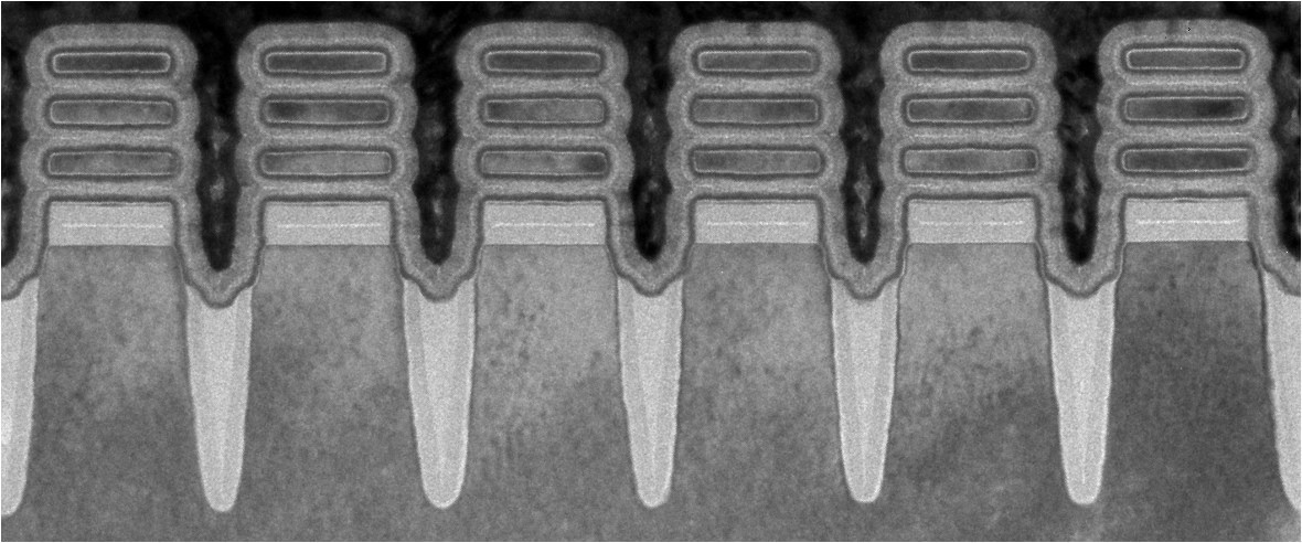
IBM Develops 2nm Devices
To continue research into single nm devices, IBM has recently announced the successful development of 2nm chips. The devices utilise a nano-sheet with a thickness of only 2nm. This enables the creation of transistors smaller than even the most advanced devices currently manufactured, such as those by TSMC.
Specifically, the new device provides an increase of 45% in performance and a 75% reduction in energy use compared to typical 7nm devices. According to IBM, the use of its 2nm nano-sheets will enable chips with 50 billion transistors that are no bigger than the size of a fingernail. Furthermore, if deployed commercially, IBM expects that the 2nm technology could see the quadrupling of battery life in smartphones, reduce global CO2 emissions as a result of reduced energy consumption, speeding up devices, and help with AI technologies by increasingly device complexity.
IBM has long been involved with the development of key semiconductor technologies. For example, IBM was the first to make breakthroughs in 7nm and 5nm technology, developed single-cell DRAM, enabled Silicon on Insulator technology, and copper interconnects on semiconductors.
"The IBM innovation reflected in this new 2 nm chip is essential to the entire semiconductor and IT industry. It is the product of IBM's approach of taking on hard tech challenges and a demonstration of how breakthroughs can result from sustained investments and a collaborative R&D ecosystem approach."- Darío Gil, SVP and Director of IBM Research.
When will 2nm devices become commercially available?
It is one thing to create 2nm devices in a lab, it is another to make it commercially viable. While some companies are concerned if devices smaller than 3nm will ever become viable, others such as TSMC are actively researching into the field to try and create smaller transistors. If research continues to be successful in the field, the development of 2nm chips can be expected around the 2023 to 2025 years.
However, while 2nm devices would enable reduced power consumption and increased computing performance, most consumer electronics would not utilise such technology. Furthermore, assuming that manufacturing devices below the 7nm node prove expensive, it may take decades for the devices besides processors and graphic cards to feature such technology. For example, STM32 manufacture their own semiconductors, but their process node ranges from 0.18um to 65nm demonstrating that sometimes, going smaller is not needed.
Read More