China’s Latest QLC Flash Memory
| 17-04-2020 | By Robin Mitchell
This week, YMTC have announced their latest FLASH memory chip, the X2-6070, which stores 1.33Tb of data with access speeds up to 1.6 Gb/s. What is QLC memory and what advantages does it have over other traditional FLASH memory architectures?
QLC Memory
Flash memory is a technology that has been around for three decades with the first proven devices dating back to 1980. Flash memory is a non-volatile storage method which means that it is able to retain data held in the memory cells even when it is turned off and is a key technology in everyday life ranging from USB flash drives, solid state drives, and microSD cards found in almost all mobile devices. While the exact operation of flash memory is somewhat complex the basic principle is simple; a MOSFET transistor has a floating gate that sits between the gate and the transistor channel. When a high voltage is applied across the gate electrons can be tunnelled in or out of the floating gate and when electrons are tunnelled into the floating gate they remain trapped. Therefore, the presence, or lack of, electrons in this gate will change the conductive properties of the transistor and thus represent a digital 1 or 0. Such technology stores one bit per transistor and each transistor is a storage memory cell thus each cell stores one bit. If more data is to be stored on a chip without increasing the X and Y dimensions of that chip additional silicon layers can be added on top of the chip (Z dimension) with each layers having memory cells. Current flash technology can see as many as 128 silicon layers which has helped give rise to high memory density applications such as solid state drives.
However, if each cell holds an analogue value instead of a digital value then each cell could potentially be made to store more data. As more electrons are stored on the floating gate the threshold voltage of that transistor changes linearly and if the threshold voltages are quantised into specific regions then each region can represent a different state. Thus, if four states can be clearly defined then that cell can store two bits (00, 01, 10, and 11). This can be taken even further by defining 16 different states which can store four bits.
Enter the X2-6070
To meet the growing demand for larger solid state archive storage YMTC, based in China, have announced the worlds largest FLASH memory, the X2-6070. This device is a 3D silicon device with 128-layers of QLC Flash memory. Each cell in the device can store 4 bits of data (and thus 16 different states) which allows it to store a total of 1.33Tb of data. The devices, which are based on Xtacking architecture, claim to operate at I/O speeds of up to 1.6Gbps and run on a VCC of 1.2V. It is believed that these devices will be fabricated at the XMC Fab facility which is one of Chinas largest silicon foundries. For smaller devices, YMTC have also announced the smaller X2-9060 which is also a 128 layer 3D memory chip but stores 512Gb instead of 1.33Tb. Currently, no data sheets have been released so device specifics are still in the dark.
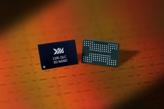
YMTC X2-6070 128-Layer QLC 3D NAND memory chip
Credit: YMTC
“As client SSDs transition to 512GB and above, the vast majority will be QLC-based. The lower read latency of enterprise and datacenter QLC SSDs compared to hard drives will make it suitable for read-intensive applications in AI, machine learning and real-time analytics, and Big Data. In consumer storage, QLC will become prevalent in USB flash drives, flash memory cards, and external SSDs.” - Gregory Wong, principal analyst of Forward Insights
Technology Drawbacks
This technology allows for dramatically increased memory sizes for the same size silicon die but it does have its drawbacks. Because flash memories pull electrons onto the floating gate via tunnelling they are somewhat destructive which results in flash memories have a maximum number of writes per cell (can be as much as 1 million but typically between 10,000 and 100,000). Flash memory technologies that employ multi-bit storage per cell suffer from this problem far worse and can have as few as 100 writes per cell. This is why these technologies are more ideal for large server farm storage (such as Youtube) where data is unlikely to be altered but needs to be stored and accessed frequently. Flash memories can be read as many times as needed but can only be written to a finite number of times. Increasing the number of bits stored onto a single memory cell also increases its access time and thus are slower memories than their single bit counterparts. This is why such memory architectures are more suited for long term storage of data (such as archives and backups).
