High-voltage GaN semiconductor breakthroughs are essential for electric vehicle applications
Semiconductors | 23-04-2018 | By Paul Whytock
According to many of the automotive and battery industry cognoscenti, all of us will be driving around in electric vehicles by the year 2030.
Whether you believe that and whether you think there will be sufficient public charging points and electricity on national grids to make such predictions an actuality is another matter.
Research and development accelerated for higher voltage chips
What is for sure, though, is the global semiconductor industry has its foot hard down on the R & D accelerator when it comes to creating high voltage chips that can cope with the demands of EVs. And there have been, and still are, some significant design challenges when it comes to creating devices that can handle switching at up to 1200Volts.
In reality, it is well recognised that it is difficult for applications beyond 650V, such as electric cars and renewable energy, to increase the buffer thickness on 200mm wafers to the levels required for higher breakdown and low leakage levels. Primarily this is because of the mismatch in coefficient of thermal expansion (CTE) between the GaN/AlGaN epitaxial layers and the silicon substrate, says research centre Imec.
Some experts say that because of the higher CTE characteristic of gallium nitride GaN, the stress during epitaxial growth, the use of 1.15mm thick 200mm silicon (Si) substrates is beneficial because it will reduce the problem of wafer warp during growth and potentially cut the risk of fracturing.
However, there can be processing problems when using thicker substrates. Fundamentally, the processing problems are compatibility issues in wafer handling that can occur in some processing tools.
Imec Technologies overcome GaN substrate technology limitations
Imec has been working with Silicon Valley-based wafer fab company Qromis and its Qromis Substrate Technology (QST) range of substrates.
According to the two organisations, CMOS fab compatible QST substrates with a CTE that matches the thermal expansion of the GaN/AlGaN epitaxial layers make 1200V buffers on 200mm substrates a possibility.
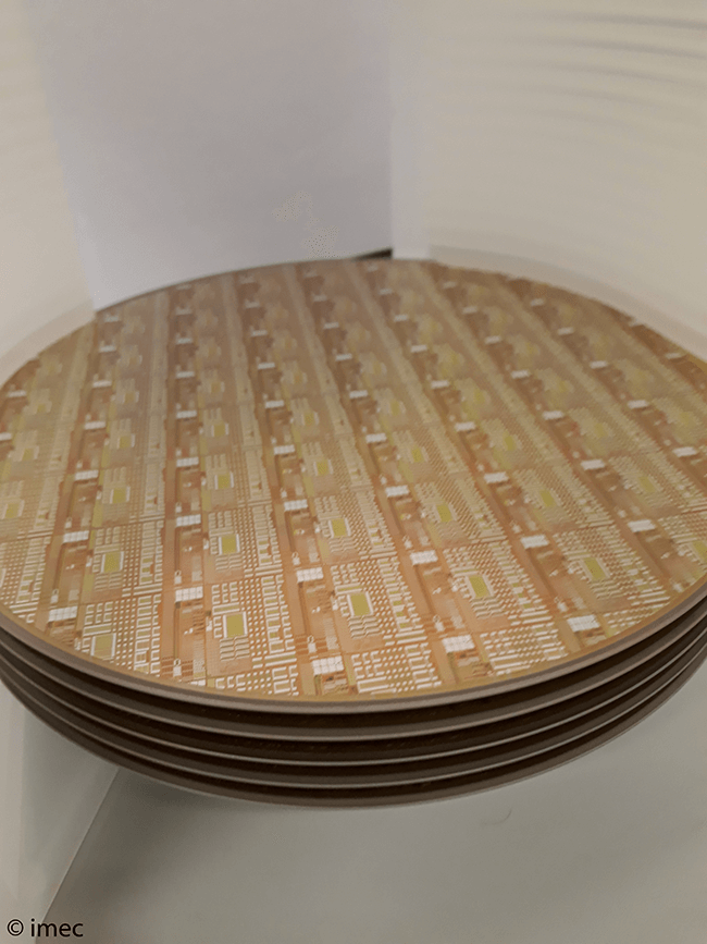
A result of the collaboration between the two organisations is the development of enhancement mode p-GaN power device GaN epitaxial layers on 200mm QST substrates with buffers grown in AIXTRON’s G5+ C 200mm high volume manufacturing metal-organic chemical vapour deposition (MOCVD) system.
Imec then ported its p-GaN enhancement mode power device technology to the 200mm GaN-on-QST substrates in its silicon pilot process and demonstrated high-performance power devices.
Conclusion
It’s reasonable to say that 200mm GaN on Si will be a dominant factor in the power device arena, and developments that look at elements like substrate technology relative to CTE, high integration of on-chip GaN transistors and quasi-vertical and vertical architectures will push performance boundaries further forward.
Read More: Are these E-mode GaN-on-Silicon power devices a World first?