Navitas Provides Complete Gallium Nitride Power Solutions
Insights | 21-02-2024 | By Gary Elinoff
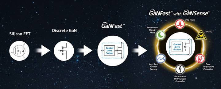
GaNFast with GaNSense. Image source: Navitas
Essential Insights into GaN Technology:
- Gallium Nitride (GaN) and Silicon Carbide (SiC) power semiconductors have many advantages over last-generation Silicon devices.
- For all its virtues, designing circuits that exploit GaN design is complex and prone to unexpected difficulties.
- Navitas Semiconductors makes it easier for engineers to exploit these revolutionary devices in their designs.
Introduction
Anticipating the upcoming APEC 2024 conference in Long Beach, CA, Navitas Semiconductor is poised to introduce a series of products designed to simplify the integration of gallium nitride (GaN) and silicon carbide (SiC) power semiconductors for manufacturers. These devices, representing the cutting-edge class of wide bandgap semiconductors (WGB), offer significant benefits, including power savings, reduced heat generation, and enhanced efficiency, all within a compact footprint. Such advancements are set to redefine the landscape of power electronics, providing engineers with the tools to create more efficient and space-saving designs.
Understanding the market adoption and practical applications of GaN and SiC technologies is crucial for appreciating their impact. For instance, Navitas Semiconductor's GaNSafe™ technology, as highlighted in their recent launch, opens up multi-billion dollar opportunities in data centers, solar energy, and electric vehicles by offering unprecedented protection and efficiency (Navitas Semiconductor). This aligns with the global shift towards more sustainable energy solutions and the increasing demand for high-performance, energy-efficient power semiconductors.
The problem is that GaN and SiC devices are difficult to work with, requiring very specific expertise not often found among digital design engineers. Indeed, engineers not well versed in power often underestimate the difficulties involved in perfecting power-based designs. While not about GaN or SiC specifically, an article published in Forbes[1] details how no less an organization than the mighty Apple floundered when underestimating the unexpected difficulties presented in perfecting power applications.
Moreover, the evolution of charging technology, as demonstrated by the widespread adoption of GaNFast chargers, underscores the significant efficiency gains and size reductions achievable with GaN technology. Companies like Anker and Xiaomi have leveraged GaN to produce compact, powerful chargers that redefine consumer expectations for charging speed and convenience, highlighting the practical benefits of GaN in everyday devices (GaNFast Media Coverage).
What’s So Special about Wide Bandgap Semiconductors?
Silicon power semiconductors can only turn on and off (switch) at speeds of up to a few hundred kilohertz, while GaN devices can switch at speeds over ten times as fast. This is enormously important to power supply designers, as power supplies require what is called filtering, and the size of the requisite filtering components sport weights and sizes that are inversely proportional to switching speeds.
Since the filtering components of a power supply represent a major portion of the power supply’s size and weight, the vast reductions made possible by using GaN power semiconductors are key selling points.
But it doesn’t end there. In power supplies, power semiconductors, as mentioned earlier, must switch on and off, and it is critical for the resistance between the device’s source and drain during the device’s “ON” state to be as close to zero as possible. This ON state resistance is widely denoted as RDS(ON).
Why is this so important? Because, as derived by Ohm’s Law, power is equal to current squared times resistance (I2R). So, any resistance between the source and drain is immediately converted to energy. This parasitic energy is doubly significant because:
- Any energy that is wasted within the semiconductor won’t be available at the output of the power supply.
- The parasitic energy generated doesn’t just disappear but rather expresses itself as heat. This requires more heat sinking, venting and other modalities to remove that heat. This, again, mandates a larger, heavier power supply, exactly what nobody wants.
Insights into Navitas’ GaN Technology
We mentioned earlier that GaN, despite its very notable advantages over Silicon power devices, is a difficult technology to implement. That’s why designers generally don’t attempt it and leave the headaches to specialists – like Navitas.
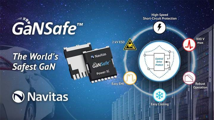
Navitas GaNSafe™ Technology. Image source: Navitas
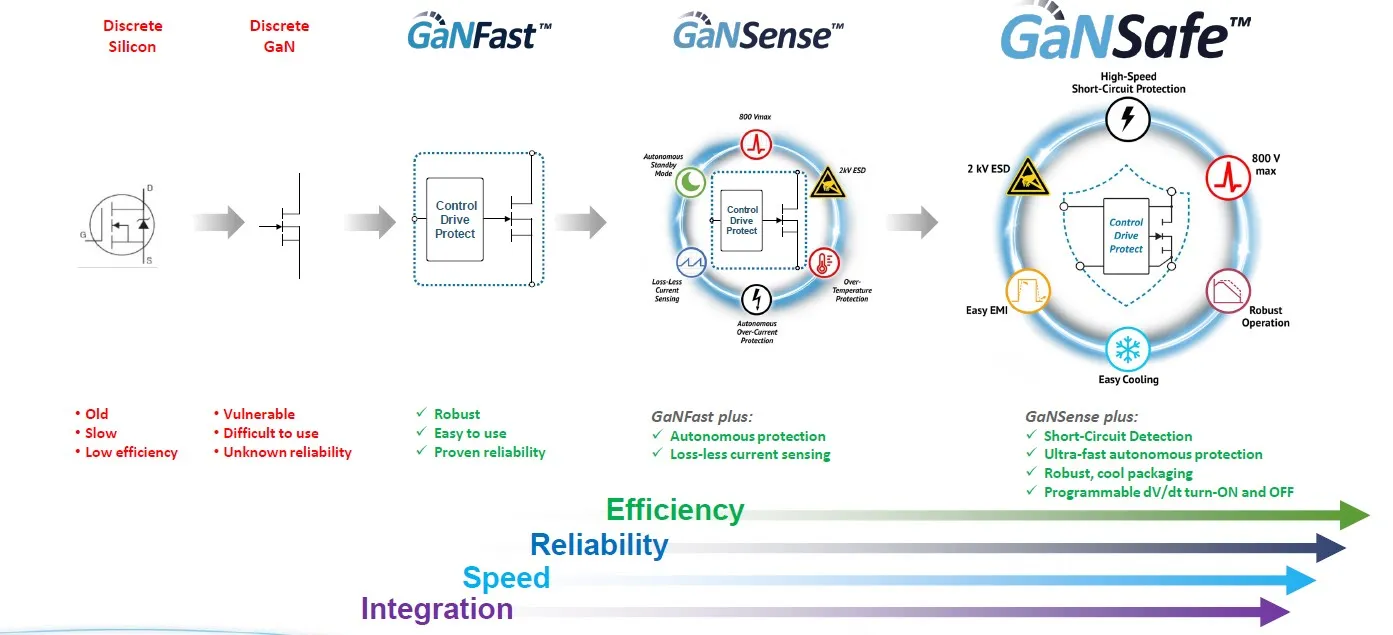
The sequence of Navitas’ GaN technology is illustrated above. From left to right, the first two illustrations contrast discrete silicon to discrete GaN devices. Next, the GaNFast illustration shows a pivotal advantage that Navitas’ GaN devices provide. Here, we see the tricky GaN device packaged with control, drive and protection circuitry all in a single package, eliminating headaches that even power supply designers are generally not equipped to handle.
The fourth segment illustrates GaNSense, which augments GaNFast with more protection and current sensing. The last illustration is GaNSafe™, which adds short circuit detection, programmable dV/dT turn-ON and OFF and other features to GaNSense.
The bottom line is that many designers can achieve this level of design sophistication with silicon chips. But even there, the parts count will soar, making for a less reliable, larger and heavier end product. With GaN., the difficulties are multiplied. That’s why savvy designers leave the headaches to experts like Navitas.
It's also important to note the critical role of E-A-T (Expertise, Authority, Trustworthiness) in the development and implementation of GaN technology. Navitas Semiconductor's collaboration with TSMC for the manufacturing of GaNSafe and GaNSense ICs exemplifies a commitment to quality and reliability, leveraging TSMC's renowned manufacturing capabilities to ensure the highest standards are met (Navitas Semiconductor). This partnership not only enhances the product's trustworthiness but also reinforces Navitas's authority in the GaN technology space.
Navitas’s GaNSafe™ and GaNSense Technology Highlighted at the APEC 2024 Conference
Looking ahead to the APEC 2024 conference in Long Beach, CA, Navitas Semiconductor is set to showcase its GaNSafe™ and GaNSense technologies, signaling a pivotal moment in power semiconductor innovation. These advancements in gallium nitride (GaN) and silicon carbide (SiC) semiconductors demonstrate Navitas's dedication to enhancing efficiency, reliability, and safety in power electronics. With the integration of sophisticated protection features and sensing capabilities, Navitas aims to tackle the challenges of wide bandgap semiconductor applications, establishing new benchmarks for the industry. This upcoming presentation is expected to underscore Navitas's leadership in the sector, illustrating how their innovative solutions are ready to transform data centers, renewable energy systems, and electric vehicle (EV) technologies, leading the charge towards a more efficient and sustainable technological future.
GaNSafe™
Navitas highlighted its GaNSafe™ technology and its special GanSense GaN Power ICs at the conference. The new line of semiconductor devices will be manufactured by the world-famous Taiwanese manufacturer TSMC. The units are targeted at applications in data centers, solar/energy storage and the electric vehicle (EV) market, with power requirements ranging from 1 to 22 kilowatts.
Navitas’s GaNSAFE Technology. Image source: Navitas
RDS(ON)s range from 35 to 98 milliohms - that’s less than 1/10 of an ohm! These units operate at potentials of up to 650 volts, with surges up to 800 volts tolerable. There is also built-in protection against electrostatic discharge (ESD) of up to 2,000 volts. The company cites two complete power products, based on GaNSafe™ GaN’s, that it builds and markets on its own.
One is a 6.6 kW 3-in-1 bi-directional EV on-board charger (OBC).
The second is the CRPS185 data center power platform, which delivers 3.2 kW. It achieves a power efficiency of over 96% over 20% to 60% load. This is in a package of 40 x 73.5 x 185 mm dimension, which works out to a power density of just under 100 w/in3. The CRPS185 meets the 80Plus Titanium power efficiency standard, which is mandatory in the EU for server power supplies.
GaNSense
The company also featured its GaNSense product line, partially summarized here. For a deeper dive, check out this overview of the NV6247 half-bridge power IC. This device consists of two GaN FETs, including complete drive, control, sensing and protection capabilities. Nabil Akel, a Navitas Sr. Staff Applications engineer, details the operations of this complete power solution in a highly informative video.
More About the GaNSafe™ Line
As illustrated below, the GaNSafe™ line includes the NV6515, NV6513, NV6512 and NV6511.
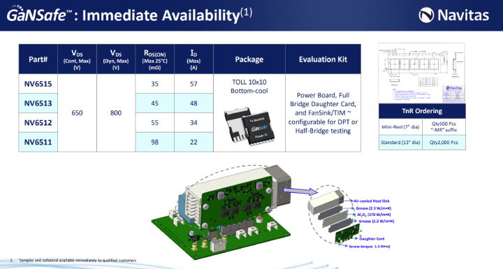
The GaNSafe™ Line. Image source: Navitas (Page 32)
Note how series members sport RDS(ON)s ranging from 25 to 98 milliohms. An evaluation board is available for engineers as they test and familiarize themselves with the GaNSafe™ line.
Navitas GaN Power lines are in Wide Use
At 650 volts maximum continuous voltage, these GaN devices are a bit short of the 800 architectures now becoming standard in EVs. However, GaNFast devices have been widely adopted by manufacturers of a wide range of charging devices.
Challenges and Opportunities
Whether it’s chargers, servers, EVs or anything else, the byword today is efficiency. Don’t waste a watt because the renewable energy revolution still has a long, long way to go. As it stands now, every extra watt means that much more fossil fuel (or, worse yet) nuclear energy must be used. The former presents many well-documented environmental hazards, and the latter portends possible Chernobyls or Three Mile Islands.
The employment of GaN technology, with its uncannily high efficiency, makes sure that as few watts as possible end up in useless, parasitic heat instead of powering the electronic devices that we all depend on so heavily today and the as-yet uninvented devices of tomorrow.
Reflecting on the broader implications of GaN and SiC technologies for sustainability, it's evident that their adoption is a key driver in reducing the environmental impact of electronic devices. The efficiency improvements and reduction in power waste directly contribute to lowering the carbon footprint of technology, aligning with global sustainability goals. This aspect of GaN technology not only demonstrates its technical superiority but also its role in fostering a more sustainable future, a critical consideration in today's environmentally conscious society.
Wrapping Up
GaN semiconductor devices can convert electrical power to different voltage potentials with far greater efficiencies than legacy Silicon devices. However, like silicon devices, GaN cannot be controlled directly from CPUs or MCUs. There needs to be driver stages and many types of protections. But there is a catch. GaN devices are tricky, and creating the complete system is out of the realm of experience for all but the most specialized of power engineers. That’s where organizations like Navitas come in.
There is also a second reason to use factory-complete components such as GaNSafe™. With everything in one isolated package, the end device has a smaller parts list. With fewer components, space and weight is saved, reliability is increased, and the manufacturing process is easier and cheaper.
And, a final aside. If just the right package for a particular application can’t be found and if the anticipated manufacturing volume is large enough, designers may just be able to convince a GaN manufacturer to modify an existing component or design a new one for specific needs.
References:
- 1 Reasons Why Apple Canceled Its AirPower Wireless Charging Mat: Analysis: https://www.forbes.com
Glossary of Key Terms:
- GaN. Gallium Nitride. A wide bandgap semiconductor that handles power levels of up to 10 kW at switching frequencies of 10 MHz and more
- SiC. Silicon Carbide. Another wide bandgap semiconductor that operates at switching speeds of under 1 MHz and handles power of about 1 MW
- RDS(ON). The resistance between the source and drain of a power semiconductor
- WGB. Wide bandgap semiconductor. The class includes GaN and SiC devices.