Innovation in Education: Korea's Semiconductor Lead
In The News | 14-08-2023 | By Robin Mitchell
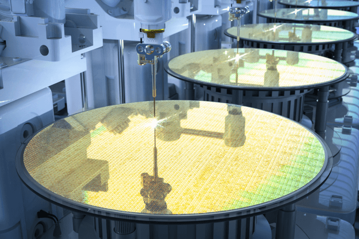
Recently, the Korean government announced that it will be launching a new limited service where students will be able to manufacture their own 500nm silicon wafers for the purpose of verification and experience. What challenges does semiconductor manufacture face with regard to education, what will the new program do, and why should this be encouraged throughout the world?
What challenges does semiconductor manufacturing face with regard to education?
Of all areas of electronics, logic design interests me the most, and if there is one thing I have always wanted to do is to get a custom silicon device made. Such a device wouldn’t be a high-end processor or a high-speed digital interface, but instead, something more trivial such as a late 1980s 32-bit processor, video signal generator, or floppy drive controller.
As this device would consist of no more than 100K transistors, it wouldn’t need to be manufactured using state-of-the-art process nodes; it could easily be done in 1um technology. And yet, despite this node having been achieved in 1984, no semiconductor service currently exists that allows for basic devices to be manufactured at affordable rates. You would think that, after all this time, making such semiconductors should be trivial and cheap, but unfortunately, this is far from the case.
Unlike PCBs, which are now a dime a dozen, even the most basic semiconductor device requires a large amount of infrastructure to produce. Everything from forming wafers to the application of special coatings requires substantial capital to set up, and because there is no market for low-end semiconductor devices, these facilities are far and few between.
To make matters worse, low-end semiconductors with 1um process nodes still require expensive masks and hundreds of process steps. This means that making just one wafer incurs a massive tooling cost, hence why semiconductors are produced in bulk.
Because of this reality, it is virtually impossible to get a custom semiconductor device developed at a low price. Some academic programs do allow for individual chips to be fabricated, but these are usually shared with other devices on that wafer, and there are rarely guarantees that the device will even function. Finally, such programs can still cost tens of thousands of pounds, meaning that unless a student has a substantial grant, getting custom semiconductors made is simply out of the question.
According to a recent report by the Korean government, the new initiative to allow students to manufacture their own 500nm silicon wafers is a step towards bridging the gap between education and industry. This program aims to provide hands-on experience and foster innovation in the field of semiconductor technology.
Korean government launches new program for manufacturing student wafers
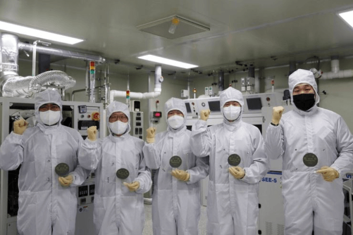 University officials and semiconductor industry leaders gather at Kumoh National Institute of Technology in Gumi, North Gyeongsang Province, on Jan. 25. Photo courtesy of Korea Times.
Recently, the Korean government announced a new program that aims to get selected student semiconductor designs manufactured to aid in the verification of designs and garnering experience in the semiconductor industry. With the increasing threat faced by semiconductor shortages, governments around the world have raced to secure their supply chains, but one supply that may have been entirely ignored is those who know how to design and make semiconductors.
The new program, which will be open to both undergrads and graduate students, will be empowered by government funding and manufactured at the Electronics and Telecommunications Research Institute at Soul National University. The process node available will be 500nm, which may be far from modern devices produced by TSMC and Intel, but plenty sufficient for student projects, and this process node also makes it easier to manufacture.
However, as such projects are expensive to run, and manufacturing facilities often have limited capabilities, only 25 teams will be selected for 2023. Fortunately, as this project runs, the selection number will increase to 150 in 2024 and over 300 by 2026.
The Korean government's initiative is seen as a pioneering effort to address the global semiconductor shortage and to nurture the next generation of engineers. By providing opportunities for students to engage in real-world manufacturing processes, the program aims to create a sustainable talent pipeline for the industry.
Why should this be encouraged around the world?
While FPGAs and hardware verification tools can be used to determine if a semiconductor is likely to work, actually building a device is by far the best method for device verification. By physically building a device, the value of the experience gained by solving real-world problems faced by semiconductor manufacturing is immeasurable. Any student who has the opportunity to create their own semiconductor device through trial and error has the capacity to excel in the industry, giving the country where they reside an outstanding advantage.
Considering the numerous challenges faced by the semiconductor industry over the past few years, it only makes sense for the West to start running more of these programs. As we said before, simply securing supply chains is only half the problem of the semiconductor issue; if there is no one who knows how to use them, what is the point in securing them?
If such projects gain popularity, there is a chance that low-volume semiconductor foundries start to open up shop, allowing engineers from all backgrounds to manufacture their own devices. This could be immensely popular in circuits that require unique ASIC functions (such as amplifiers and specific logic control) and may even help to spark a new industry of low-end custom semiconductors. Maybe in the future, semiconductor devices could be bought in a similar fashion to cheap PCBs, with Gerber files uploaded, paid for, and sent out for just a few dollars.
