Creating Wood Electronics via Laser-Induced Graphitisation
| 20-07-2022 | By Liam Critchley
Many people and companies worldwide are looking toward sustainable solutions for a greener future while trying to maintain the same level of living standard and technological advancement. Electronics often come under fire as wasteful material, not necessarily from the energy that we consume, but more so from the levels of waste (e-waste) that can be left behind if they are not appropriately recycled (or recycled at all in the case of some components).
We all know that traditional electronic systems are by and far the most advanced and efficient systems and will be sticking around to underpin the main technological advances in our society. Still, there has been a growing interest in creating ‘green electronics’ made from more sustainable materials that involve more environmentally friendly manufacturing methods.
In the realm of sustainable and green electronics, many small devices have primarily been created using nanocellulose as the primary material. However, despite widespread interest, it requires a lot of energy and chemicals to process nanocellulose into functional electronic devices. So, from a commercial perspective, other materials are being investigated; a material that has gathered some significant interest in the last few years is wood.
Not all electronics are going to be made ‘green’ because the range of properties and functionalities in conventional electronics is too great to shift to natural materials―and you would never be getting high heat generating systems made from natural materials that could catch fire. However, as we start to look towards a more connected Internet of Things (IoT) world, where many small-scale devices offer a way of capturing and monitoring data, there is the potential to use greener electronics in more remote locations where conventional electronics can sometimes struggle.
This is especially true for remote monitoring applications where the monitoring devices only have a limited lifetime of use, so rather than being left to pollute the local environment after use, a more sustainable wood (or other natural material) device would be able to decompose back into the earth and not leave behind waste. While wood has typically been difficult to work with, it does offer a way of biodegrading after use in these scenarios, and a team of researchers have now taken a laser-induced graphitization (LIG) approach to try and create functional wood electronic devices.
Using Wood for Electronics
Wood fits the bill when looking for more sustainable materials because it is a natural, renewable, and biodegradable material that can store carbon dioxide. While wood is not itself conductive, it offers a stable platform for electronic systems to be integrated on (much like the synthetic silicon-type materials in conventional electronics) because it is lightweight and has high mechanical strength.
However, wood has not been as widely explored because its lack of intrinsic electrical conductivity makes it harder to connect components on the surface, even though it is an excellent structural material. Several different attempts at coating the surface have been trialled, but graphitizing the surface (and just below) to create graphite and graphene-like materials could open up new ways of utilizing wood in a more active capacity for electronics―i.e., by offering a way of electrically connecting components as opposed to just supporting them.
As we look towards remote IoT applications, where the devices could get left in the field after use, the biodegradability of all organic systems (including the graphite/graphene materials) could offer a way of naturally disposing of the device once used. Even in health monitoring (as sensors) and haptic devices (touchscreens and displays), devices that can be naturally degraded could offer a way of reducing the amount of e-waste produced nowadays.
Using Laser-Induced Graphitisation (LIG) to Build Wood Electronics
Laser-induced graphitization is a process that is used to convert a range of organic and inorganic precursor materials into electrically conductive and porous carbon materials with a controlled morphology. In some instances, it is used to create graphene derivatives, while other times, it is used to create graphite-like materials. The process of creating graphene-like materials in this way gathered a lot of attention a few years ago when James Tour from Rice University fabricated conductive laser-induced graphene patterns onto toast and other foodstuffs.
Wood has typically been a challenging material for LIG processes because it has low thermal conductivity. Because LIG processes are a small and concentrated source of heat, the surface of the wood can undergo a significant level of thermal degradation before the bulk does, and this can cause surface cracks and shrinkage of the wood to occur. However, high temperatures of around 1200-1300°C are still required to create conductive graphite-like materials on the surface of the wood. So, finding a way to induce the graphitization of the wood’s surface while not causing permanent degradation has been sought.
A team of researchers from Switzerland and Germany have now been able to achieve this with a conventional CO2 laser under ambient conditions, thanks to the use of an aqueous bio-based iron-tannic ink coating inspired by historical iron-gall ink. The iron ink provided a catalytic surface for the graphitization reaction to occur, facilitating large-scale areas (100 cm2) of porous graphite-like conductive foams. In addition, the iron coating also enabled the graphitization without causing any ablation or thermal degradation to the wood substrate itself.
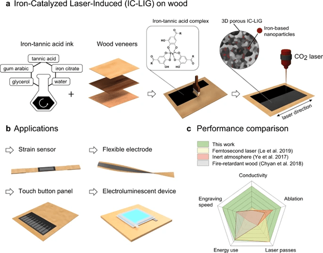
a Schematic representation of the IC-LIG process. The substrate (e.g., a wood veneer) is coated with an iron-tannic acid ink (the inset shows a simplified structure of the iron-tannic acid complex contained in the ink, see also Supplementary Fig. 1). The ink-coated wood veneer is then treated with a CO2 laser to achieve IC-LIG (the inset shows a schematic of the resulting 3D porous iron-carbon composite). b Proof-of-concept applications demonstrated in this work for IC-LIG structures on wood veneers: a strain sensor, a flexible electrode, a touch buttons panel, and an electroluminescent device. c A radar plot comparing the performance of our IC-LIG with other previously published LIG approaches in terms of process parameters (faster engraving speed, lower energy use, only one laser pass needed) and quality (higher electrical conductivity, lower substrate ablation) of the resulting LIG materials.
The graphite-like areas were fabricated onto different wood materials―including wood with a 450 µm thickness―and were found to be highly conductive, with an electrical conductivity of more than 2500 Sm-1. This is an order of magnitude higher than the previous highest literature value of 400 Sm-1. Beyond this, the engraving speed of the iron-catalyzed LIG process was up to 35 times faster than other methods, and because it only required the use of a single moderately powered laser, the energy consumption was lower than other LIG approaches as well.
To demonstrate how the graphite-wood electronic devices could be used in different applications, the researchers put together a series of devices to show the application potential of these sustainable electronic systems. The devices included a durable strain sensor for health monitoring, a flexible electrode for motion tracking, a capacitive touch panel for human-machine interfaces, and an electroluminescent device using the LIG as an electrode.
There’s still a way to go before we may see more sustainable electronic systems being used in real-world applications but choosing to use LIG with wood―and to do it without damaging the wood― could offer some interesting bases to carry on from in terms of future research, promoting wood as a viable green electronics option in a field where nanocellulose has typically dominated so far.
Reference: