DC/DC Conversion Topologies and Techniques
Educational | 27-07-2021 | By Mark Patrick
Power conversion is an essential function in many applications, from infotainment systems to battery-powered IIoT sensors. Several basic switching mode topologies are commonly used for DC/DC and AC/DC power conversion.
The specific type used depends on the voltage levels required and the amount of power needed. This article investigates the basic concepts of power conversion and showcases the popular DC DC converter topologies used for discrete and module-based designs. The article also covers the critical aspects of isolation and voltage regulation.
AC/DC & DC/DC Converter Topologies and Power Conversion Is Everywhere
Conversion functions are in most of the technology that we use today. Take smartphones, for example.
It most likely contains a lithium battery, which has a nominal 3.7 V output voltage. The phone's many ICs and associated functions may operate at different voltage levels, the most popular being 1.8 V, 3.3 V or 5.0. Power conversion functions take the 3.7 V and convert it to the appropriate voltage level, whether above or below the battery's nominal output voltage.
Another similar example is the humble USB power bank sold in their millions to help us recharge our tech on the go. Again, it will use a single lithium pouch cell providing 3.7 V, and a DC/DC converter will increase the output to supply the standard USB 5 V output.
Smart speakers, televisions, laptops, and domestic appliances all need to convert the supply voltage to a level the internal circuitry uses. AC/DC and DC/DC conversion methods include two distinctly different techniques; linear or switching.
The linear method was widely used in the past for mains-powered equipment but suffered from the need for bulky components such as a large transformer and smoothing capacitors. Linear regulators get used in some specialist DC/DC conversion tasks, but most applications today employ a switching regulator approach.
A switching-based DC DC converter topology relies on storing energy in an inductor or capacitor. Unlike a linear approach, a switching regulator can provide an output voltage greater than or less than the input voltage.
Figure 1 highlights the basic concept of a switching mode DC/DC converter.
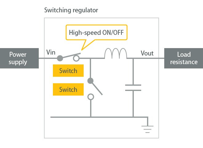
Figure 1 - Functional block diagram of a DC/DC converter (source Murata)
A PWM signal is applied to a semiconductor device as a switching drive signal. The duty cycle (mark-to-space ratio) and frequency of the PWM input directly impact the conversion efficiency, load regulation, and output voltage. Essentially, the PWM and the switching semiconductor create a charge pump circuit to store energy in an inductor or capacitor during the ON cycle.
This energy is released and rectified during the OFF period of the PWM signal. Regulation of the output voltage is applied to the PWM signal. Input-to-output isolation is achieved by using a transformer as the inductive element in addition to a capacitor. Over the years, several DC DC converter topologies have become popular and are now briefly explained.
Popular DC/DC Converter Topologies
The Step-Down Buck DC/DC Converter Topology
An asynchronous buck converter topology converts an input voltage to a lower output voltage, for example, 5 VDC to 3.3 VDC. A simple explanation of the circuit is highlighted in Figure 2.
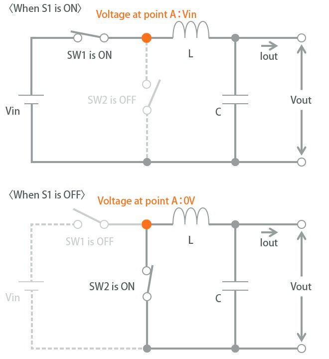
Figure 2 - The primary function of a buck converter (source Murata)
In Figure 2, SW1 is usually a transistor driven with a PWM signal, and SW2 is a diode. When SW1 is closed or ON, current flows through the inductor, storing energy. When SW1 is OFF, energy is released as the current flowing through the diode represented by SW2 and provides an output voltage.
The output voltage of the buck converter depends on the duty cycle of the switching PWM signal, as illustrated in figure 3.
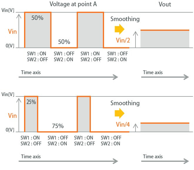
Figure 3. The impact of duty cycle on the output voltage (source Murata)
The diode is replaced in a synchronous buck topology with another switching element, typically a FET. It is fed from an out-of-phase switching signal. FETs typically offer lower forward resistance, reducing losses.
The Step-Up or Boost Converter
As the name suggests, in a boost converter, the output voltage is higher than the input voltage.
How much higher depends on various factors, but for most practical purposes, the maximum is up to five times the input voltage. A factor of up to three times is more viable to achieve good output voltage regulation. See Figure 4.
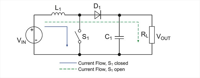
Figure 4 The basic concept of a boost converter (source Recom)
Compared to the arrangement of the buck converter illustrated in Figure 2, the switching transistor S1, inductor L1, and the diode D1 (was a switch in Figure 1) are placed in slightly different positions.
Energy is stored in L1 when S1 is ON, and when switched OFF, the energy is added to the input voltage already across the input capacitor and passed to the output capacitor.
Buck and boost converters use very few components, and this approach ensures they achieve high energy efficiency, typically up to 97 %. Both the buck and boost converter topologies highlighted above are not isolated. That means any input voltage can appear at the output.
If the DC/DC converter is powered from an AC line power source, a failure could cause the AC line voltage to appear at the output with potentially fatal consequences.
Many applications require galvanic isolation between the input and output, medical and healthcare applications, for example. For instance, one way of achieving galvanic isolation, where the ground connection is not common, in a switching regulator is to use a transformer; an example is the isolated flyback converter (see Figure 5.)

Figure 5 - A simplified schematic of an isolated flyback converter (source Wikipedia)
The Isolated Flyback Converter
In an isolated flyback converter, the transformer is both the energy storage inductor and provides isolation. This topology is perhaps the simplest of all DC/DC converters with a low component count.
Applications are typically restricted to low-power applications ( < 50 W) and those that can tolerate relatively high ripple currents. A transformer introduces primary to secondary losses, so most flyback converters struggle to achieve better than 90 % energy efficiency.
However, unlike buck and boost topologies, the use of a transformer permits increasing or reducing the turns ratio to achieve a broader range of potential output voltages. Also, additional secondary windings can be used to deliver multiple output voltages.
Push-Pull, Half Bridge and Full-Bridge Converters
Push-pull, half-bridge and full-bridge converters are examples of other isolated switching topologies in use. The Push-pull arrangement uses two switching devices, sharing the current between them and suiting higher power applications.
This topology uses split centre-tapped primary and secondary windings, requiring a more expensive transformer. The half-bridge and full-bridge topologies are similar to the push-pull but only need a single primary winding. A half-bridge uses two switching devices, and the full-bridge uses four - see Figure 5.
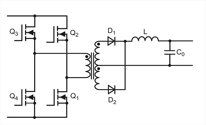
Figure 6 - A full-bridge isolated DC/DC converter simplified schematic
Output Regulation
Aside from basing a DC DC converter design on a specific topology, deciding how to regulate the output voltage is an important consideration. Achieving tight regulation of the output across all load conditions is especially important for processors with rapidly changing dynamic compute workloads.
Feeding back the output voltage to the PWM switching function to change the duty cycle must be achieved quickly and precisely. Today, most DC/DC converter control ICs incorporate this function, a task that is easily achieved in a non-isolated topology.
However, maintaining input to output isolation involves extra components, adding to the BOM cost. Popular isolated feedback methods include using an extra transformer or an optocoupler. The need for additional components increases not only the BOM cost but also the PCB space requirements.
Furthermore, in today's space-constrained designs, PCB space needs to be kept to a minimum. Also, alongside BOM cost, the more components used in a design, the more complex the component sourcing and logistics challenges become. Using more components also impacts the reliability of the end product.
DC/DC Converter ICs and Modules
A recent innovative solution uses primary side sensing to provide a much simpler method of regulation. During the flyback "OFF" phase, the controller IC senses the reflected secondary output via the transformer. An example of a "no opto" flyback controller IC is the Maxim MAX17687 - see Figure 7.
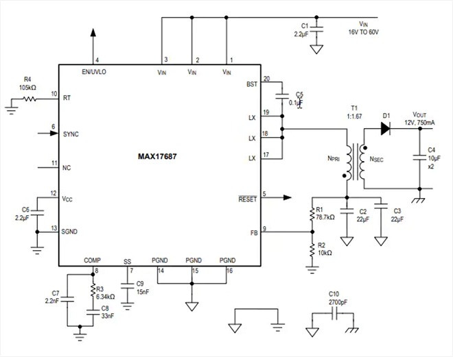
Figure 7 - An example no-opto minimal component count flyback converter IC used to create a 12 V / 750 mA output from a 16 V to 60 V source - the Maxim MAX17687 (source Maxim)
The MAX17687 controller incorporates two on-chip MOSFETs capable of driving a primary peak current of 3.2 A. Using the primary-side sensing technique, the output voltage is regulated within +/- 1.2 %.
The IC's PWM frequency is programmable between 100 kHz and 500 kHz, and conversion efficiency is typically better than 90 %. An example of a complete flyback DC/DC converter module is the open-frame, through-hole mounted isolated Murata UWS-Q12 series. Modules offer an attractive alternative to designing a discrete DC/DC converter.
Firstly, a significant amount of design effort is removed from the development process, potentially saving considerable engineering time. It is also beneficial from a BOM perspective since it reduces the component count and simplifies component logistics.
Another aspect is that modules are typically already certified for EMC/EMI compliance and conformance to medical safety standards, further simplifying product approvals. The compact 91 % efficient UWS-Q12 series offers the popular nominal single output voltages of 3.3 V, 5 V, 12 V, 15 V, or 24 V and can deliver up to 54 Watts from a 9 V to 36 V input voltage.
A comprehensive set of self-protection features, such as input under-voltage and over-temperature, are included.
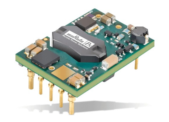
Figure 8 - The Murata UWS-Q12 (source Murata)
A convenient method of replacing inefficient legacy linear regulators, the Traco TSR 1.5E series is a drop-in 1.5 A part that uses a buck step-down non-isolated topology to achieve efficiency up to 97 % and accommodates a wide range of input voltage.
Devices within the series provide 3.3 VDC (7803 replacement), 5 VDC (7805 replacement), and 12 VDC (7812 replacement). TI has adapted the buck converter topology with its DCS-Control technology (direct control and seamless transition).
The modified DCS topology achieves significantly better transient response, regulation, and ripple characteristics than a synchronous buck approach. TI supplies the converter both as a controller IC, the TPS6282x, and a converter module with an integrated inductor.
Figure 9 illustrates the functional block diagram of the non-isolated buck converter module with integrated FETs and inductors.
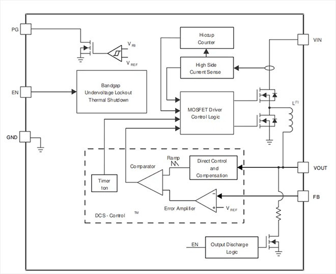
Figure 9 - Functional block diagram of the TI TPSM82821 step-down buck converter module featuring the TPS6282x controller IC (source TI)
Power Conversion Made Simple
This article investigated some of the more popular DC/DC power conversion topologies and highlighted some product examples. Converter ICs are a popular space- and BOM-efficient method of achieving DC/DC conversion.
Low-power converter ICs that integrate switching transistors or FETs are extremely popular in many industrial, commercial, and consumer products.DC/DC converter modules that incorporate the controller IC, inductor, and all additional components are the simplest to integrate into an end product and the easiest to procure.