Researchers Demonstrate New Memory Technology Utilizing Atomically Thin Layers
| 25-05-2021 | By Robin Mitchell
Recently, researchers have developed a new memory technology that takes advantage of atomically thin layers. What challenges do current memory technologies face, what have the researchers developed, and are monolayers the future of electronics?
What challenges do modern memory technologies face?
Without memory, computers simply cannot function. For example, the results of operations can’t be stored for later use nor can they be fed back into the computer for further manipulation and condition checking. However, no singular memory technology can be used in a modern computing system as different memory technologies have different advantages and disadvantages.
The three main memory properties are speed, cost, and size; a memory technology can pick any two of these but will suffer on the third. For example, DRAM is low cost and fast, but it suffers from a poor memory density (it takes an entire bank of them to get a few GB). Hard disks are low cost and provide massive storage densities, but their slow speed makes them inappropriate for any instantaneous work (i.e. they are ideal for long-term data storage). Finally, flash memory offers a very small footprint that is low in cost, but FLASH is slow (compared to DRAM), and has a maximum number of write operations before failing.
No matter how hard scientists try, finding a memory technology that offers a low-cost solution that can operate at speed and provide great density seems to be impossible. However, if researchers were to find a memory that could do everything, memory technology would become “Universal Memory” where the cache, RAM, and long-term data are located.
Researchers Develop Fast 2D Non-Volatile Memory
Recently, researchers from the Chinese Academy of Sciences’ Institute of Physics in Beijing have created a new memory technology utilizing atomically thin layers stacked on top of each other to create a non-volatile memory cell. The physical construction of the memory cell uses a layer of indium selenide semiconductor, a boron nitride insulating layer, and graphene layers that sit above a wafer of silicon dioxide and silicon.
Each layer is atomically thin, and while typical materials use either ionic or covalent bonds to retain their structure, the new device uses van der Waals forces. This means that the layers are stuck together in a similar fashion to sticky tape, and the resulting interactions between the layers result in unique properties.
The memory cell is a floating-gate transistor meaning that when a strong voltage is applied across the device, electrons get trapped in the floating gate layer. From there, the conductivity of the channel below the transistor depends on the field strength of the trapped electrons.
According to the researchers, the device can be programmed with voltage pulses as small as 21ns making it almost as fast as typical DRAM used in computers. As such, the new memory technology is 5000 times faster than typical FLASH memory which opens up opportunities in the memory industry.
However, the researchers also stated that the new memory technology might be able to store multiple bits in a single cell. For example, instead of simply holding a 1 or a 0 to represent two different logic states, the new memory technology may allow for multiple states to be stored in the form of varying levels of trapped electrons. As such, the 2D structure of the cell can partly overcome its memory density disadvantage when compared to FLASH memory, which can have as many as 100 layers of bit storage per cell.
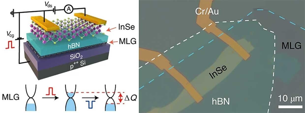
Image courtesy Nature Nanotechnology
Why are nanolayers becoming a point of interest?
Before the development of nanometer-scaled devices, almost all electronics operated on macroscopic physics; electrical current is the flow of electrons, resistance is impurities in a structure, and valves operate because a voltage potential blocks the path of electrons from the cathode to the anode. However, as the size of electronic components reduces, macroscopic physics models begin to break down, and strange effects such as quantum tunnelling become more prominent.
While such quantum effects are generally undesired, they are highly sought after in nanomaterials. Nano layers such as Graphene and Indium Selenide exhibit unusual properties that are not present in standard solid materials. When these layers are combined with each other, they can produce materials with extraordinary electronic properties. In the case of the researchers from China, their memory device operates 5,000 times faster than typical FLASH memory.
Furthermore, exploiting such small structures allows researchers to continue the shrinking of electronic devices to the atomic scale. As such, electronic devices will continue to become more powerful, use less energy, and become smaller than ever.
Read More
