New Solution Processing Methods for Organic Electronic Devices
| 07-04-2020 | By Liam Critchley
The field of organic electronics has seen a lot of interest in recent years. On the whole, the performance and efficiency of organic electronic devices are not typically as high as inorganic-based electronics. However, their unique properties – especially their flexibility, conformability and thinness compared the more rigid inorganic materials – have seen them being used for specific applications and in areas where the properties of conventional inorganic-based electronics are not suitable. Some of the key applications where organic electronics are currently used include flexible solar cells, wearable electronics, organic light emitting diodes (OLEDs) and in flexible transistors, but the list is continually growing.
The Area of Organic Electronics
As the name suggests, it is electronic devices that are fabricated using organic materials, such as polymers and small organic molecules. This in contrast to many conventional electronic devices which tend to use inorganic materials, such as silicon, indium tin oxide (ITO) and ceramic materials, to name a few of the most common examples. The differences in the materials stems from fundamental chemical principles, where many inorganic materials tend to be metal or metal oxide based, but organic materials are made up of carbon-based materials.
One of the reasons that organic electronic devices don’t generally have as high efficiencies is due to inorganic materials being much more electronically conductive – especially the ones chosen for electronics which use highly conductive metals in their chemical makeup. However, there are a range of conductive organic molecules out there, especially conductive polymers, which can be processed and fabricated into electronics devices. Aside from their increased flexibility, organic electronics are typically cheaper to make, can be fabricated using simple technology (such as printing methods), are often lighter than inorganic components, and the carbon backbone of the organic molecules can often be easily tailored and tuned using conventional organic reactions, meaning that the properties can be tweaked to suit the application. So, what they lose in efficiency, they make up for in other areas.
Solution Processing Methods
One of the most promising methods for producing low-cost organic electronics are solution processing methods. Solution processing methods are material deposition methods where the materials are deposited from a solution on to the fabrication surface. However, as it stands, a number of different solution processing methods are required to fabricate a device. This not only includes different solutions, but it can that a lot of different fabrication equipment is required to fabricate the different parts of the device and stick them all together. So, while the processes themselves may be of low-cost, the manpower and time required to use so many different approaches are too high for some applications.
One of the widely used processing and patterning methods in this space is photolithography. While it is highly effective, photolithography requires multiple steps where sections and masked and exposed to light to remove unwanted parts of the material. There is a range of other imprinting and patterning methods out there which are crucial for organic electronic devices, and all have similar issues where sections need to be protected due to a lack of chemical stability (organic molecules tend to be less stable to heat, pressure, harsh chemicals etc than inorganic materials). So, there has been a lot of work going in to solve these issues.
New All-Solution Processing Methods
One of the main ways touted to overcome these issues is to use photo-crosslinking processes to make the organic polymer networks more chemically robust. Photo-crosslinking the materials, if done correctly, is an approach that can increase the thermal stability of the materials (crosslinked polymers tend to be stronger in many property departments compared to non-crosslinked polymers). There have been a number of polymers and organic devices created using this approach, however, Jeong Hong Cho and colleagues across Korea looked to take this method one further and adapt it for the patterning and stacking of multiple functional materials.
The all-solution processing approach builds on these principles and has been used to fabricate thin-film patterns of solution-processable semiconductors, gate insulators, and conductors, which in turn were used to fabricate a fully patterned polymer thin-film transistor (PTFT). Research has shown that azide-based molecules can facilitate photo-crosslinks in the relevant polymers; and an azide known as 4Bx was used because it is applicable with many different solution processed materials, ranging from polymer semiconductors to metal nanoparticles, and it doesn’t degrade the electrical properties of the polymer once incorporated (something which other azides can do as they change the morphology of the polymer film).
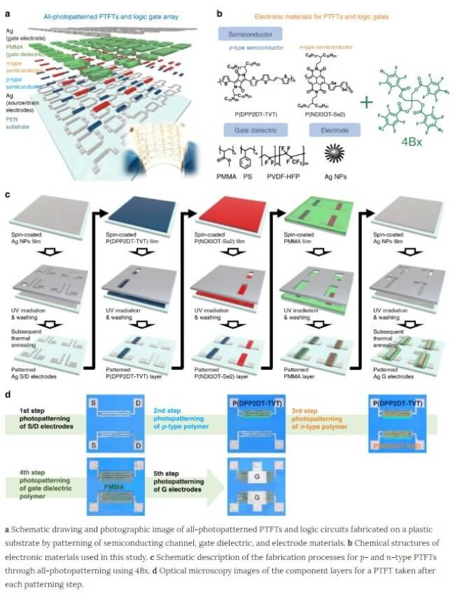
Credit: Cho J. H. et al, Universal three-dimensional crosslinker for all-photopatterned electronics, Nature Communications, 11, (2020), 1520
The researchers were able to complete the device through a series of solution processing methods and photolithography patterning methods, which sped up the time and ease of the fabrication over other methods, as there was no need for multiple pieces of equipment. The main reason why it could be processed in this way was due to the 3D structure of the crosslinker and its versatility to be used with a wide range of solution processable materials – i.e. it could be added in at all the different fabrication stages to crosslink with the layer being patterned/deposited, therefore the fabrication process could be performed in the same processing environment throughout, regardless of the layer. The different layers were then processed, patterned and stacked on top of each other meaning that a complete device could be completed with relative ease.
One of the benefits of this method aside from all the processing stages being fabricated in series, is that the crosslinked networks can be simply formed using ultraviolet (UV) rays, the fabricated devices are inherently resistant to harsh chemicals (due to the enhanced nature of the crosslinked materials) and the process retains the natural electronic and structural properties of all the materials within the device, making it less likely to be prone to stability issues down the line. While this is just one processing method for making organic electronics, it can be used to make large-area organic electronic devices; and any new methods that improve the manufacturing capabilities is good for the industry as a whole as it offers new options towards the large-scale manufacturing of different organic electronic devices.