How 2D Perovskite Photovoltaics Could be Improved
| 30-04-2020 | By Liam Critchley
There are several materials out there which are used to fabricate the junction of a solar cell. While some of the thin and flexible solar cells, you will see are organic in nature, most solar cells to date are inorganic in nature. Of these inorganic solar cells, there are two general types – those which are wafer-based and those which are made up of thin films. In today’s advanced manufacturing environment where many materials and methods are available to create thin films, thin-film solar cells are becoming a widespread emerging class of photovoltaic (PV) devices. Within the class of thin-film solar cells lie a whole host of different materials, including various nanomaterials, thin crystalline and amorphous materials – with perovskite materials being one specific type.
Perovskite Materials and Their Role in Photovoltaics
Perovskite is a term that classifies a group of materials which have similar chemical compositions, morphology and characteristics. There are many different materials which fall into this material category, but all have the chemical structure of A2+B4+X32-. In simple terms, the A and the B refer to two different cations – with A having an ionic charge of 2+ and B a charge of 4+ – both of which are linked by an anion that bonds to both cations. In more simple terms the structure can be shortened to ABX3. Originally, perovskite only referred to calcium titanate (CaTiO3) as it was the first known example of this ‘perovskite structure’, but the category has since been expanded to include all materials with the same type of structure.
Perovskites have been touted as a useful material for the junction of solar cells for several reasons. Overall, the perovskites used can absorb wavelengths of light across the whole electromagnetic spectrum. They have a fast charge separation of active charge carrier species, long charge carrier distances and can be tuned (chemically) with relative ease, and the production of the active perovskite materials in solar cells is relatively cheap and easy (even if the overall device is expensive). All these factors have led to the fabrication of highly efficient solar cells.
Issues with 2D Perovskite Materials for Photovoltaic Applications
As it stands, 3D perovskite materials are the most prevalent in solar cell applications because their power conversion efficiency (PCE) has reached up to 25.2%, which is very high. However, we haven’t seen their usage as much as other materials due to the solar cell being of a much higher cost than other materials (such as silicon or gallium arsenide) because of the electrodes required in the device (not necessarily the active perovskite materials). 2D perovskite materials have also shown much promise for solar cell applications, especially as they are much thinner than their 3D bulk counterparts. However, they currently suffer from a completely different set of issues that will first need to be remedied before they can be used commercially.
It is thought that the stability of 2D perovskite solar cells will surpass that of 3D perovskite solar cells. However, the PCE is not as high as 3D solar cells. The PCE is one of the drivers of perovskite solar cells, and it is thought that the lack of a high PCE in 2D perovskite solar cells is due to when the electrons in the junction cascade after photoexcitation. Typically, the electrons will cascade very soon after photoexcitation. This means that the time it takes for the energy carriers to travel across the junction is much longer due to an increased thickness in the neutral region of the junction. This leads to the energy carriers relaxing, cooling and being separated much quicker than is optimal. Because many charge carriers relax at the junction, there are less charge carrier combinations across the junction, which leads to open-circuit voltage loss and a reduction in the PCE. Additionally, there tends to be an energy disorder across 2D perovskite films which leads to an uneven distribution of energy across the junction. Still, it’s thought that these issues could be remedied by optimising the material structure and how the perovskite structure crystallises when being formed.
The Potential for 2D Perovskite Improvement
It is thought that the limiting factor of charge carrier relaxation is due to the charge carriers with a small bandgap, as these tend to cool and separate first. The crystallisation of perovskite materials, when formed, can produce different sized crystals within the material, and this intrinsic defect is thought to be a significant contributor to the uneven energy landscape within 2D perovskites.
It has been discovered that the material structure and crystallisation mechanisms are highly dependent on how the organic cations are distributed in the solution that is used to make the perovskite material. Knowing this, Mingjian Yuan and colleagues in China looked to understand further how small tweaks could yield much more optimal 2D perovskite materials for PV applications using a series of computational and experimental methods.
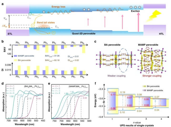
After various computational trials into seeing how the perovskite structure could be optimised, it was chosen that the lead iodide-based perovskite being trialled should contain a thin film of meta-(aminomethyl) piperidinium (MAMP) to provide a flatter band structure and a more homogeneous energy profile across the perovskite. It was found that the occurrence of the MAMP ligand regulated the crystallisation kinetics during perovskite formation, which decreased the number of defects in the material and reduced the degree of energy disorder across the device, leading to increased stability and PCE.
The research has shown that through careful planning, spotting the key issues and using computational approaches to optimise the solution before physically fabricating the device, could be the way to go for many perovskite materials. This approach of using MAMP has shown that many of the issues with 2D perovskites can be negated, opening the possibility for them to be used in future devices. In terms of this specific device, the PCE was 16.53%, which is a significant advancement on other 2D perovskite solar cells and was found to be more stable than when other solutions have been trialled. It’s early days yet, but it presents an opportunity to optimise future 2D perovskite materials for solar cell applications.