Development of a Nanoscale Triboelectrification-Gated Transistor
| 12-03-2020 | By Liam Critchley
The evolution of nanotechnology in last decade or so has brought about technological advances that were not previously possible in the electronics space. Aside from trying to induce more functionality (or multifunctional properties) into a device, one of the biggest issues in recent years has been the ability of a device or component (regardless of the type) to maintain a high efficiency or achieve a greater efficiency while being miniaturised. Scaling down bulk materials to small dimensions can only be achieved to a certain point before the process becomes either impractical or unfeasible from an economic perspective.
Recent times have seen a shift from a top-down miniaturisation approach to a bottom-up approach where ultra-small nanomaterials are built up atom by atom and integrated into a device (either directly or via a transfer). This has led to electronic devices being fabricated that are much smaller in nature while still possessing the same levels of efficiency, if not better.
However, one area where there is still some struggle is in the interaction between nano-enhanced devices and a human/surrounding environment, particularly where physical monitoring and information acquisition is concerned. Granted, nanoscale sensors and some Internet of Nano Things (IoNT) devices are effective as non-contact devices, but there is still a drive to establish active interactions between a nanoelectronic device to obtain information directly. One promising area is tribotronics which is the intersection of machine elements and electronic components to create an active tribological system that can interact with its surroundings.
Triboelectric Nanogenerators (TENGs)
There have been a number of solutions proffered over the years, with many more appearing recently because nanoelectronic devices are becoming more popular and commercially feasible. Out of all the solutions devised over the years, triboelectric nanogenerators (TENGs) have become a common choice because they can convert mechanical motions into electrical outputs using triboelectrification inductions. However, TENGs on their own are more suited to energy storage applications but they can be coupled with other materials, such as semiconductors, to create a range of tribotronic devices. While a lot of progress has been made in these areas, most of the devices are only capable of interacting with an external stimulus at a macro level, but there has not been much exploration towards active interactions at the nano level.
Developing a Nanoscale Triboelectrification-Gated Transistor
Research has now been developed by Chi Zhang et al into a different tribotronic device known as a nanoscale triboelectrification-gated transistor (NTT) and builds on previous work where TENGs have coupled with other materials but can be used for nanoscale interactions. Given the small size of the device, two different nanocharacterisation techniques known as atomic force microscopy (AFM) and scanning Kevin probe microscopy (SKPM) – which is a technique that also relies on AFM principles – were required to investigate the surface properties of the device, as this is the area of the device which was designed to interact with its surroundings.
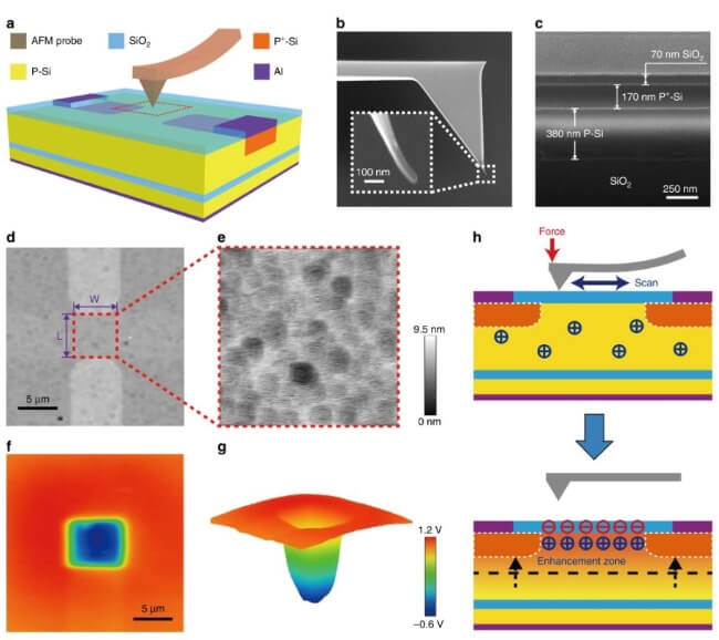
Overview of the nanoscale triboelectrification-gated transistor (NTT).
a Schematic illustration of the NTT gated by nanoscale triboelectrification. Scanning electron microscope (SEM) images of the (b) atomic force microscopy (AFM) tip and (c) NTT in cross-sectional view. AFM images of (d) the top SiO2 surface in tapping mode and (e) the rubbed area above the channel region in contact mode. f Surface potential distribution of the top SiO2 layer after regionally rubbed by the AFM tip measured in scanning Kevin probe microscopy (SKPM) mode. g 3D image of the measured surface potential distribution. h Schematic working principle of the NTT gated by nanoscale triboelectrification.
Credit: Zhang C. et al
The device features a sandwiched layer at the bottom of the device, where a layer of silicon dioxide forms a channel between two p-doped silicon layers. Aluminium and p-doped silicon pads were deposited on top, followed by a final layer of silicon dioxide. The probe of the AFM instruments was crucial for determining how the device interacted physically at the nanoscale as the very small tip is typically only 10 nm, so could be used as a tool for seeing if an interaction with external stimulus can be recorded at the nanoscale.
To do this, the AFM tip was used to manipulate the surface of the device so that it can tune the carrier transport across the surface of the device. The interaction between the tip and the device surface led to a nanoscale triboelectrification effect on the surface of the device which simulated the effects that could occur in a real-world environment with an external stimulus. This approach could then be used to investigate the effects that changes in the contact force, scan speed, contact cycles, contact region and charge diffusion have on the properties of the NTT device.
The movement of the AFM tip above the surface of the device enabled the manipulated nanoscale triboelectrification to serve as a rewriteable floating gate with different modulation effects. Therefore, the device fabricated by the researchers is essentially a nanoscale triboelectric modulation on top of a transistor that can provide direct interactions for electronic devices with external stimuli; and could have implications in nanoelectromechanical systems (NEMS), human-machine interfaces and flexible electronics.
Characteristics of the NTT
The NTT has a similar structure to conventional metal oxide semiconductor field-effect transistor (MOSFETs) without the top gate electrode. The interaction with an external stimulus caused an electron transfer process to occur from the stimulus (in this case the tip) to the surface of the device. This caused the inner silicon dioxide channel to generate an inner electric field which attracted holes (positively charged carrier species which are the opposite of electrons) and repelled the electrons in the p-doped silicon layers. This causes an enhancement zone to form which increases the drain current and enables the interaction to be defined and recorded.
It was found that the nanoscale triboelectrification could also be manipulated in the presence of an applied electrical field. In the presence of such fields, more electrons are transferred from the physical stimulus to the device and this results in an enhanced internal electric field that attracts more holes towards it. The result is that the device is highly tuneable. So, while the device created is something that could be coupled with other electronic components in the future, the research also provided some insights into how tribotronic devices work when stimulated and the different ways in which the device can be manipulated and tuned to suit a particular application.