7 Things To Consider About Nanotubes In Electronics
| 16-12-2019 | By Gary Elinoff
Carbon nanotubes have been the “technology of the future” since the days of the Buckyball in 1985. With the demonstration of a field-effect transistor made of carbon nanotubes that can operate in the 100 GHz range, that future is now. The technology has “graduated” from university labs. It now is being pursued by industrial corporations and the military, who are interested in short-term results, and not long-range possibilities. But first, a bit of background.
1- What are Buckyballs?
They are named after Buckminster Fuller, inventor of the geodesic dome. Buckyballs or Fullerenes are nanoparticles composed entirely of carbon. They have a spherical structure, similar to Fuller’s geodesic dome, hence the name. The picture below is a representation of a buckyball composed of 60 carbon atoms
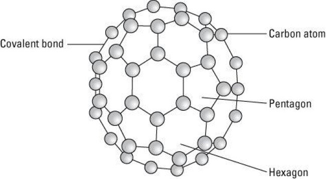
Image source: Understanding Nano
Originally, carbon nanotube structures were renowned for their strength. That strength comes partially from their structure, the way each atom held in place by three others. The other source of strength is the solid covalent chemical bonds between each atom in the structure. It is also to be noted that they are unusually good conductors of electricity.
2- What is Graphene?
Like buckyballs, graphene is an allotrope of carbon, This means that, like diamonds, the substance is simply another way that carbon atoms can combine. Graphene is the thinnest structure known, with a depth equal to the radius of a carbon atom. For this reason, graphene is said to be a two-dimensional sheet. It is also transparent, bendable, and, oh yes, far stronger than steel.
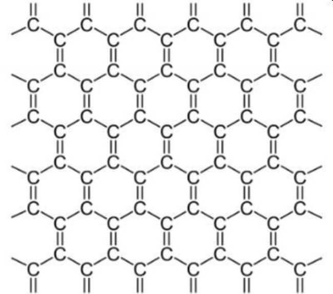
Graphene.
Image source: Graphene-info
3- What are Carbon Nanotubes?
Finally, if a single sheet of graphene is “rolled” into a tube, the result is a carbon nanotube. Oftentimes, one or both ends the tube is “capped” with one half, or a hemisphere, of the buckyball structure, described earlier. There can be either single wall or multi-wall carbon nanotubes. The latter can be thought of as tubes within a tube. The illustration below is a representation of an uncapped double-walled nanotube.
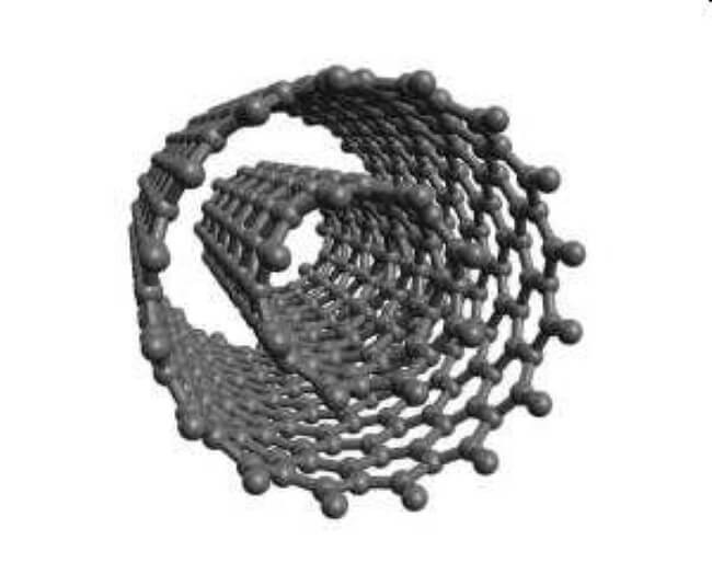
A double-walled carbon nanotube.
Image source: Ctimaterials
4- The Problem with Today’s Transistors
Especially now, with the advent of 5G, the name of the game in electronics to today is speed. Even somewhat beyond 5G, there is a need to operate the superfast speeds ranging from 30 to 300 gigahertz (GHz), aka the millimetre wavelength area. The fastest semiconductors available today are made from gallium arsenide (GaAs). But there is a major problem with GaAs technology. And that is, that it is hard to “bond”, or deposit GaAs to silicon substrates, which are the major building blocks for semiconductors. This has led to two separate sub-optimal solutions
• Don’t use GaAs, and instead employ CMOS, which is not as good at superfast speeds as GaAs
• Use a separate GaAs chip for the high-speed subsections of a product. This takes up space, requires interconnections, leaves room for error and makes manufacturing more difficult.
5- Carbon Nanotubes in Electronics
One of the most important facts relating to carbon nanotubes is that they can be configured as semiconductors, just like silicon. That means that they can form the basis of semiconductors, with some very important characteristics. Carbon nanotube tunnels have such tiny radii that they can be thought of as one dimensional – no width or height, just length, the perfect pathway for mobile electrons. Recently, at the Carbonics corporation, scientists have developed a Field Effect Transistor (FET), based on a carbon nanotube variation with a gate length of 110 nanometers. This novel device can operate at 100 GHz. This is beyond the practical limit for similar silicon-based devices, which top out at about 90 GHz.
6- Depositing Nano Carbons on Common Substrates
Carbonics’ major step forward involved single-walled carbon nanotubes (SWCNTs). Most importantly, they were able to successfully deposit this carbon nanotube variety onto mainstream substrates that are the backbone of today’s electronics industry. These substrates include silicon, silicon-on-insulator (SOI) and quartz. They can even be melded onto flexible materials, which is another very hot new electronic modality recently commercialized.
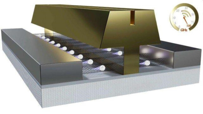
Carbonics’ Carbon Nanotube Technology.
Image source: BusinessWire
The image above is an artist’s animated version of what is happening on an atomic level. The bright spots are electrons, and we see them travelling through the nanotubes, which serve as “superhighways” for the travelling electrons Carbonics has dubbed its deposition technology “ZEBRA.” Through this method, it has proven possible to deposit a dense concentration of carbon nanotubes onto the range of computer chip substrates described above. There are two important value propositions for this achievement:
• This will allow super-fast 100 GHz subsystems to exist on the same IC wafer as the more pedestrian CMOS process. No longer will two separate chips be needed.
• 100 MHz is only the start of the story for carbon nanotube devices.
7- Carbon Nanotube Technology is now ready for Primetime
The military puts a high premium on ultra-high frequency devices that are compact and treat every last microwatt as a precious commodity. This is why they were early-stage backers of this breakthrough technology. “This milestone shows that carbon nanotubes, long thought to be a promising communications chip technology, can deliver,” said Dr Joe Qiu, a program manager at the Army Research Office. “The next step is scaling this technology, proving that it can work in high-volume manufacturing. Ultimately, this technology could help the Army meet its needs in communications, radar, electronic warfare and other sensing applications.” The original backers of IC circuitry a half-century go were the US military. As such, it is hardly surprising that the same group is avidly pursuing this next giant step. And, as per Carbonics’ CEO Kos Galatsis, “With this exciting accomplishment, the timing is ripe to leverage our CMOS-compatible technology for the 5G and mmWave defence communication markets. We are now engaged in licensing and technology transfer partnerships with industry participants, while we continue to advance this disruptive RF technology.”