Chiplets: Reducing Costs and Accelerating Chip Design
Insights | 02-10-2025 | By Gary Elinoff
Key Things to Know:
- As monolithic chips become ever larger and more complex, monolithic manufacturers face lower yields and increased costs.
- It is now possible to “mix and match” pre-manufactured, monolithic chiplets from which to build the equivalent of a system on a chip (SOC).
- Chiplet systems can often take up less board space than equally complex SOCs.
Introduction
Software IP licensing is a contractual agreement where a software owner grants a third party the rights to use their software, usually in exchange for a fixed price or loyalty. It is also possible to license chip designs, including physical layout, and the customer can then engage a foundry to actually build the chip. Famously, ARM creates microprocessor designs and licenses them to others to incorporate in their own Systems on a Chip (SOC).
In both these cases, it frees SOC designers from the task of “reinventing the wheel”. Why design a memory, CPU or analog functionality when tried and true IP can be bought for far less than the cost of developing it in-house?
But for monolithic ICs, this methodology has its limits. The chances that a new monolithic IC will fail in manufacturing increase with the number of transistors and interconnects it sports. The manufacturing process itself will be more difficult and expensive.
The solution, in many cases, is for separate chips, or Chiplets, to separately incorporate various functions. These chiplets are designed, manufactured and tested by vendors and sold to external system designers, with the costs shared by the customers. It is similar to the concept of engine manufacturers, buying the various engine parts from an array of manufacturers.
So why buy a design when you can buy a fully designed, tested and ready to rock physical subsystem?
What Exactly are Chiplets?
Chiplets themselves are single, monolithic chips. There are, for example:
- CPU chiplets
- Memory chiplets
- Analog chiplets
- I/O chiplets
Part of the utility of chiplets is that engineers can pick and choose. For example, they may buy the CPU from one manufacturer, memory from another and I/O from a third. They can mix high-speed components from one source and low-power devices from another.
This provides designers with enormous flexibility. They can save money by utilizing an inexpensive, low-power I/O chiplet if I/O needs are sporadic. They can opt for a fast, expensive, power-hungry CPU device only if it will be needed.
How are Chiplets Mounted?
Chiplets are themselves monolithic dies, but they are not mounted on a larger silicon die, as sometimes thought. Rather, they are mounted onto packages which themselves mate with the PCB. Three possible arrangements are illustrated below.
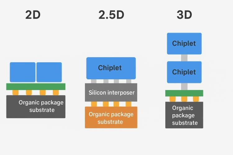
Picture provided by AI analysis
- 2D, or two-dimensional, illustrates a number of chiplets mounted on organic package substrates.
- 2.5D shows what is called a “silicon imposer” sandwiched between the chiplet and the substrate.
- 3D refers to one or more chiplets mounted on top of each other.
As illustrated, the chiplet is mounted either on the substrate or the silicon imposer. Then the imposer or the substrate, as the case may be, is mounted onto the system’s PCB, usually via BGA (Ball Grid Array) solder balls.
Chiplets are tiny, and their height is even smaller than their length and width dimensions, so they can be thought of as two-dimensional devices. The silicon imposer adds just a bit to the height, so its use inspires the 2.5D nomenclature. 3D refers to the more significant third dimension that is manifested by the stacking of two or more chiplets vertically. Whether for 2D, 2.5D or 3D arrangements, the height dimension is still very small compared to the length and width dimensions
It has been demonstrated that chiplet systems, especially the 3D types, actually take up less board space than equivalently complex monolithic SOCs.
The purpose of the silicon imposer, if it is used, is to speed communication between the various chiplets by providing denser, shorter, cleaner wiring. Silicon imposers do add to cost, and they can also impose thermal management issues.
How do Chiplets Communicate with each other?
As with the various subsystems within monolithic ICs, chiplets don’t just communicate with the system as a whole; they also communicate with each other. Standards are being adapted by the chiplet industry to make this possible, and UCIe™ (Universal Chiplet Interconnect Express) now appears to be the most dominant.
As defined by the UCIe Consortium[1], “UCIe™ (Universal Chiplet Interconnect Express™) is an open specification that defines the interconnect between chiplets within a package, enabling an open chiplet ecosystem and ubiquitous interconnect at the package level.”
Board members include “Alibaba, AMD, Arm, Advanced Semiconductor Engineering, Inc. (ASE), Google Cloud, Intel Corporation, Meta, Microsoft, NVIDIA, Qualcomm Incorporated, Samsung, and Taiwan Semiconductor Manufacturing Company”.
The standard defines:
- Physical Layer (PHY). Specifies the physical connections and electrical interfaces between the chiplets.
- Die to Die Adaptor Layer. As defined by Synopsis[2], “The adapter layer takes care of link management functionality as well as protocol arbitration and negotiation. It includes the optional error correction functionality, which is based on a CRC and a retry mechanism.”
- Protocol Layer. Again, as per Synopsis[2], the protocol layer defines the rules and conventions for data exchange, including command sets and response formats. This layer ensures compatibility between chiplets from different manufacturers.”
Open Standards
Open standards like UCIe are of great value to both manufacturers of devices like chiplets and the designers who use them. They present an example of a virtuous cycle. As manufacturers adhere to a standard like UCIe, there will be a wider range of devices built to that standard available to designers. As more engineers buy these units, the manufacturers will make more and more devices available over a wide range of purposes and price points.
This will prevent designers who work with chiplets from being locked into a manufacturer that employs an odd standard for which few others build chiplets. In essence, UCIe allows designers to benefit from a multi-vendor ecosystem, where designers can choose chiplets from any manufacturer that adheres to the standard. Thus, if the designer of a chiplet system needs, for example, a faster memory or a more powerful CPU, a replacement will be readily available, with minimal modification.
Providers of Chiplets in the UCIe Ecosystem
These include:
- AMD
- Intel
- Qualcom
- TSMC
- Samsung
- Arm
- AyerLabs
Illustrated below are the AyarLabs[3] TeraPHY Optical I/O Chiplets.
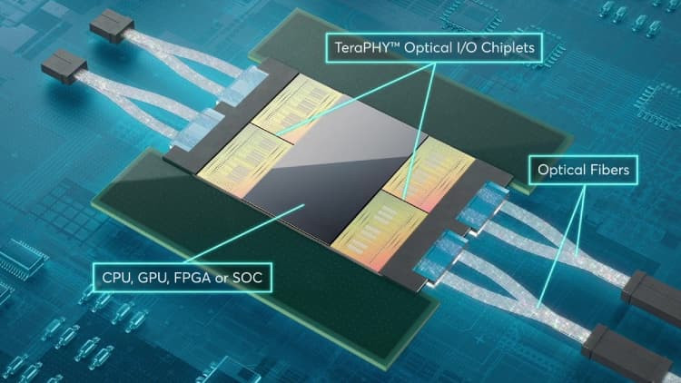
TeraPHY Optical I/O Chiplets. Image source: A Look Inside In-Package Optical I/O (00:29)
As per the company, when combined with Ayar’s SuperNova multi-wavelength light source, up to 1000 times the bandwidth using only 1/10 the power of standard electrical I/O.
Wrapping Up
As designers heap more and more complexity onto monolithic ICs, there is a greater opportunity for die failure. If the design is broken up into smaller pieces, i.e. chiplets, there will be far fewer failures due to complexity.
The emergence of standards such as UCIe is encouraging a chiplet universe that enables system designers to choose chiplets for different purposes from an ever-expanding variety of manufacturers. And if changes need to be made.
The emergence of standards such as UCIe is enabling a chiplet universe that encourages system designers to choose chiplets for different purposes from an ever-expanding variety of manufacturers. And, if changes need to be made, if a better I/O or memory chiplet becomes available, changes are easy to accomplish.
Challenges and Opportunities
Die-to-die communication may not be as fast as communication within a monolithic chip. Additionally, design verification can become a sticky problem. Along the same vein, systems designers don’t always have access to what’s going on “under the hood” of the commercially available chiplets that they order.
While the UCIe standard is gaining steam, not all the players are on board as yet.
Security can be a major issue, with multiple chiplets sourced from multiple vendors.
Most seriously, heat dissipation can be a major problem, especially in 3D systems where multiple chiplets are stacked one on top of the other.
References
Glossary of Terms
- IP (Intellectual property). Creations of the mind, including computer hardware or software, that the possessor has exclusive rights to, including the right to license it to others.
- SOC (System on a Chip). A computer chip contains many subsystems, including CPU, memory, analog functionality and I/O needed to comprise an entire system.