Cambridge GaN Devices: MOSFET Ease with GaN Power
Insights | 28-02-2024 | By Gary Elinoff
![]()
CGD’s new GaNs, like MOSFETs, can be driven easily. Image source: CGD
Essential Insights into GaN Technology:
- Gallium Nitride (GaN) semiconductors offer enormous advantages over traditional MOSFETs, including far faster switching speeds on lower ON resistances.
- End products that successfully incorporate GaN are far more electrically efficient than those employing last-generation MOSFETs
- The engineering required to implement designs using GaN technology is daunting, especially the difficulties involved in driving the GaN transistor itself. These difficulties are a significant barrier standing in the way of the exploitation of this important breakthrough technology.
- Cambridge GaN Devices (CGD) makes it possible to use standard, non-specialized MOSFET drivers, greatly simplifying the process.
Introduction
Wide bandgap semiconductors such as GaN are fast becoming the technology of choice for power applications. One reason is that GaN devices can switch on and off at speeds ten times as fast as legacy MOSFETs can. This means that the inductors and capacitors that make up the filter can be proportionately smaller, resulting in smaller and lighter end products.
When the GaN device switches ON, the resistance between the device’s source and drain (RDSON) is far lower than MOSFETs. This results in less energy being uselessly expended within the semiconductor, creating useless and harmful heat, requiring heat sinks and venting, again adding size and weight.
As per Andrea Bricconi, chief commercial officer of Cambridge GaN Devices (CGD): “GaN is now accepted as a reliable and proven technology that is able to deliver high efficiency and power density simultaneously. Datacentres, with their insatiable need for power, are an obvious application for GaN.” [1].
Indeed, the need is greater than many realize, as Giorgia Longobardi, CEO of CGD, points out that: “With datacentres now demanding 100kW per rack and predicting even more in the very near future, power system designers are looking to employ GaN devices in new architectures.”[1].
Indeed, with the advent of AI and its enormous requirements for power, the needs will only become more pressing.
The exponential growth in data center power demand, driven by the surge in AI and digitalisation, places a premium on energy efficiency. CGD's focus on GaN technology for data centers is timely, addressing the critical need for power systems that can support the future of computing while minimizing environmental impact. Their contributions at APEC 2024 highlight the role of GaN in shaping next-generation power solutions.
With these trends in mind, CGD will be highlighting its new 650 V GaN HEMT ICeGaN™ H2 single-chip eMode family of GaN power semiconductors at IEEE’s Applied Power Electronics Conference (APEC), which took place from February 25-29 in Long Beach California.
CGD’s H1 and H2 Series of Power GaNs
At the APEC show, CGD showcased its H2 and its H1 series of Power GaNs. The overriding goal of CGD was to provide a versatile series of Power GaNs that will enable designers to:
CGD's presentation of the H1 and H2 series at APEC 2024 underscores their commitment to providing versatile and efficient GaN solutions. These series exemplify the practical application of GaN technology in enhancing product performance while adhering to sustainability goals. By facilitating the transition from older technologies to GaN, CGD is at the forefront of driving innovation in power electronics.
- Easily update existing products, replacing last generation MOSFETs with modern eMode (enhanced mode, normally OFF), GaN devices.
- Design GaNs into new products with a minimum of hassle
CGD's innovative ICeGaN™ technology is a game-changer in addressing the inherent complexities of GaN transistors. By enabling these high-efficiency devices to be driven with the simplicity akin to Silicon MOSFETs, CGD is not only democratizing advanced power semiconductor technology but also paving the way for its widespread adoption across a multitude of applications. This breakthrough is instrumental in overcoming the traditional barriers to GaN implementation, fostering a new era of energy-efficient and compact electronic solutions.
CGD’s Innovation – Power GaN devices that are as Easy to Drive as MOSFETs
The Achilles' heel of Power GaN is that they are hard to control, and most specifically, they are hard to drive. CGD’s IceGaN™ devices do not need specialized drivers, but rather, they “can be operated like a Silicon MOSFET without the need for special gate drivers, driving circuitry, or unique gate voltage clamping mechanisms.” [2]
The introduction of ICeGaN™ by CGD marks a pivotal shift in addressing the complexities of driving GaN devices. This innovation not only simplifies the design process but also enhances the reliability and performance of GaN-based systems. It's a testament to CGD's expertise in GaN technology and their ability to deliver practical, cutting-edge solutions to the industry.
Members of the new family are 650 V devices driven by standard drivers at 20 to 22V. Also, with built-in Miller clamps and 3 V threshold voltages, designers are freed from the tricky, time-consuming requirement to provide negative gate voltage to keep the device in the OFF state when it’s supposed to be OFF. The units are packaged in low-profile, low-inductance DFN packages. A Kelvin pin is incorporated for optimized high-frequency, low-noise operation.
All family members provide built-in current sensing. There is no need for an external resistor, so the unit can be connected directly to ground. This draws away heat, lessening the need for heat abatement.
A Deeper Dive into CGD Technology
As described by Peter DiMaso in Electropage’s CGD video[3], an important point about IceGaN™ devices is that they include an interface circuit to the eMode GaN. It is this interface, built into the monolithic chip, that enables it to work from a standard MOS driver with a minimum of engineering intervention.
The reason why this is so important is that driving GaNs is a complex, difficult process that even most power engineers are unfamiliar with. Even if the expertise is available, the amount of design time required will be impractical for all but the largest product runs.
The diagram below illustrates CGD’s concept.
![]()
CGD’s ICEGaN™ Transistor. Image source: Electropage's CGD Video[3] (Minute 0.33 of video)
The advantages of this architecture include:
- Ease of use
- Lower system cost
- Scalability
- A more robust gate
- Better system performance
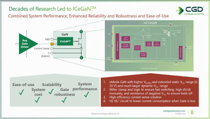
![]()
Inside CGD’s ICEGaN™ Transistor. Image source: Electropage's CGD Video[3] (Minute 1.23 of video)
The device includes an internal Miller clamp, eliminating the troublesome need to provide a negative voltage to the gate. Also, note the built-in current sense.
The practical implications of GaN's superior performance characteristics are profound, extending beyond mere technical specifications to real-world applications. From more efficient power supplies that reduce energy consumption to smaller, lighter electronic devices that contribute to sustainability, the advantages of GaN technology are setting new standards in the electronics industry. CGD's pioneering work in this field is not just about advancing technology but also about driving the kind of innovation that meets the demands of modern society for greener, more efficient solutions.
Applications
As described by CGD’s Peter Chomsky in his video ICeGaNTM Advantage in Applications[4], we first learn that the name ICeGaN actually stands for “Integrated Circuit eMode GaN”.
There are two series of IceGaN devices, H1 and H2, with four members each. A key difference is that the H2 family includes NL3 (no load, light load circuitry). As the name implies, NL3 allows the device to draw only very low power when the output current is at a minimum. The specifications of both series of devices are summarized below.
IceGaN’s H1 and H2 series. Image Source: ICeGaN[TM] Advantage in Applications.[4] Minutes: 9:05 of Video
The devices are targeted at applications including low-powered phone chargers, mid-power 350- to 500-watt laptop chargers as well as solar inverters.
Application and Evaluation
As described in the ICeGaNTM Advantage in Applications video, the company supplies numerous application boards to aid the designers in understanding and applying the H1 and H2 series of eGaNs.
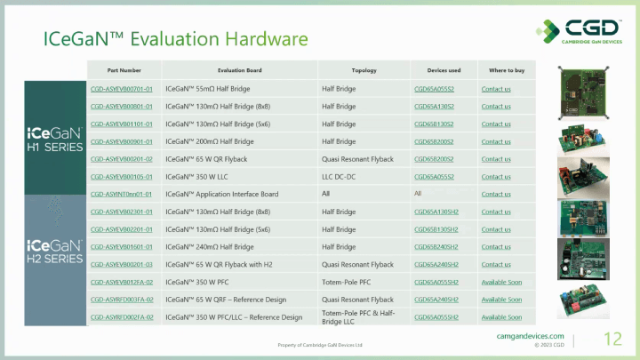
Evaluation Boards for the ICeGaN power semiconductors. Image source: The ICeGaN™ Advantage in Applications (Minute 11:30 of video)
Another Important Class of Wide Bandgap Device
Silicon Carbide semiconductors (SiC) are, like GaN, a class of wide bandgap semiconductors. They can handle more power than GaN can, but their switching speed is somewhat slower, making them important components of different types of higher-power applications.
Challenges and Opportunities
Power semiconductors play a central part in all modern electronic devices. They are the key components making cleaner energy and green electronics a reality. As pointed out by CGD[5], ICeGanTM is uniquely suited to the task of reducing CO2 emissions and reaching net zero goals by 2050. High electron mobility transistors (HEMT), such as GaN devices, make it possible to build power conversion devices with efficiencies in the area of 99%, going a long way toward achieving this vital goal.
In addition to saving space and weight, GaN devices save power. Their adaptation will serve to reduce the carbon footprint of all electronic devices and go a long way toward achieving sustainability, which is a key goal of governments worldwide.
Wrapping Up
GaN power semiconductors have numerous advantages over MOSFETs, but designers face significant challenges in exploiting this innovative technology. The engineering challenges are complex and specialized, but CGD’s ICeGanTM devices include, within their monolithic construction, interface circuitry that will greatly reduce the design tasks of engineers tasked to produce power converters of all types.
With IceGaNTM, much of the interfacing tasks are expertly handled once by CGD, as opposed to many times by downstream engineering organizations. This in itself may not directly contribute to energy efficiency, but it most certainly enhances what might be termed “engineering efficiency” in that the same engineering needs to be done only once.
References:
- Cambridge GaN Devices Addresses Challenges of Datacentres and More at APEC 2024: https://camgandevices.com/en/p/cgd-attend-apec2024/
- Our Technology: https://camgandevices.com/p/technology/
- Electropage’s CGD Video: https://www.youtube.com/watch?v=zGymKmLajBc
- ICeGaN Advantage in Applications: https://www.youtube.com/watch?v=iNMCojFn_20
- CGD: https://cms.camgandevices.com/uploads/CGD_voiceover_6b09f69c9d.mp4
Glossary of Key Terms:
- GaN. Gallium Nitride. A wide bandgap semiconductor that handles power levels of up to 10 kW at switching frequencies of 10 MHz and more
- SiC. Silicon Carbide. Another wide bandgap semiconductor that operates at switching speeds of under 1 MHz and handles power of about 1 MW
- HEMT. High electron mobility transistors, aka wide bandgap semiconductors, such as GaN and SiC.