Whitepaper: The Benefits of LDS for RF Applications
Educational | 18-12-2023 | By Youssef Laamimat
KYOCERA AVX's latest whitepaper, written by Field Application Engineer Youssef Laamimat, presents an in-depth look at Laser Direct Structuring (LDS) technology, a significant advancement in manufacturing complex 3D circuits for electronic devices. This technology streamlines the design and production of intricate components, especially in RF applications such as antennas, offering substantial benefits in terms of reduced assembly costs and enhanced performance. The whitepaper thoroughly explains the LDS process, from the initial stages of injection moulding to the detailed steps of laser activation and metallisation. It highlights the key advantages of LDS, including design flexibility, precision, and its positive environmental impact, making it a crucial technology in the current landscape of electronic manufacturing and RF component production.
The growing prevalence of electronic devices presents a challenge to numerous industries and markets. Addressing the industry's need for lighter and more compact components, LDS stands out as an excellent choice. In addition, it accelerates prototype production and streamlines time-to-market. Laser Direct Structuring (LDS) technology is a revolutionary approach offering a streamlined and efficient process for creating complex 3D circuits on a myriad of substrates. LDS technology is ideal when more curves are needed or less 3D volume is available. In RF applications such as antennas, this allows the manufacture of highly intricate designs, reduces assembly costs of having the antenna outside the device, and enhances performance while maintaining small form factors. This whitepaper by KYOCERA AVX outlines the LDS process, benefits, and key considerations, outlining its pivotal role in streamlining complex designs.
What is Laser Direct Structuring?
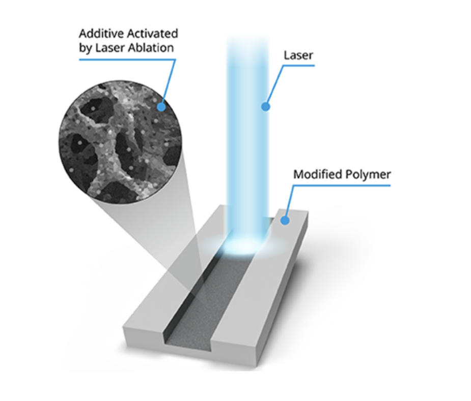
LDS is a process in which a conductive trace is inscribed directly on an injection-moulded plastic. Compared to traditional technologies, like stamped metal or flexible printed circuits, the key benefit of LDS technology is that entire 3D structures can be manufactured, offering the flexibility to integrate complex mechanical designs in miniature 3D shapes. The fundamental principle behind LDS is the ability of lasers to modify the surface properties of resins. LDS-specific resins are designed using additives, which undergo a chemical transformation when exposed to a laser, rendering them conducive. A precise structure can be developed by strategically directing the laser over a moulded resin, then the structured plastic can be plated with metals, thus creating electronic traces.
Understanding the LDS Process
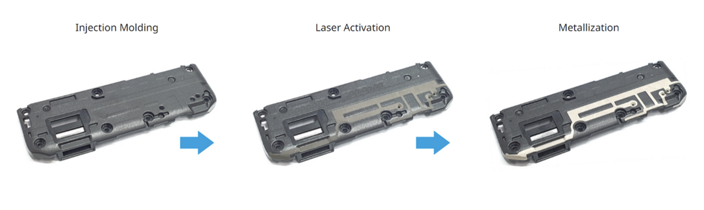
LDS consists of three main phases: injection moulding, laser activation, and metallisation, followed by additional steps, such as surface finishing and final product inspection. Below is a closer look at each of these operations and the final steps of the process:
Understanding the Controlled LDS Process
Step 1: Injection Moulding
The process begins with designing and fabricating the desired three-dimensional component with an LDS-capable thermoplastic blended with a metalorganic compound. Upon exposure to the laser, this compound decomposes, leaving behind a catalytic seed layer, which makes subsequent metallisation possible. KYOCERA AVX leverages a plastic material doped with additives specially developed for laser structuring and cross-linking. This technology allows the use of hot temperatures during the soldering process.
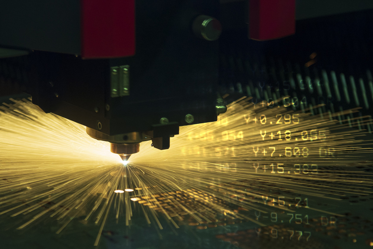
Step 2: Laser Surface Activation and Structuring
To facilitate metallisation on plastic surfaces, a specialised chemical additive is blended into the plastic material used for injection moulding. Laser activation triggers a chemical reaction, forming fine metal particles on the laser-treated area of the injection-moulded parts. Laser activation consists of the following processes:
- Laser Selection: A laser with a suitable wavelength and power is chosen to interact with the plastic's additive. Infrared lasers are commonly used for surface activation.
- Design Transfer: A computer-aided design (CAD) model of the intended circuitry is input into the laser system. KYOCERA AVX provides flexible and quick turn-around services of geometric 3D design in prototyping and mass production of LDS products.
- Laser Activation: The laser scans the plastic substrate according to the CAD model, and as it travels across, it activates regions where circuitry needs to be formed. The additive in the plastic decomposes to create nucleation sites. In addition to the metal nuclei, a rough surface can be formed on the laser-treated portion of injection moulded parts, ensuring excellent adhesion between the metal layer and plastic material during metallisation.
Step 3: Electroless Plating / Metallisation
Metallisation, achieved through electroless plating, creates metal traces on the laser-treated surfaces of injection-moulded plastic components. Here, the moulded component is immersed in an electroless plating bath. The bath, typically a copper or nickel solution, adheres to the activated regions, gradually building up a conductive layer. No electrical current is required for this deposition, as the chemical reaction is driven by the catalytic regions created during the laser structuring.
The thickness of the copper plating depends on the duration of the parts remaining in the plating bath. A layer ranging from 12 to 15 micrometres (um) is suitable for RF applications over 400 MHz and can prevent RF skin depth and effect issues. Once the desired copper thickness is achieved, the parts undergo an electroless nickel plating, typically ranging from 1 to 2 um. This nickel layer serves the purpose of corrosion protection. Optionally, a 0.1 um electroless gold plating can be added to the nickel layer. This additional gold layer enhances soldering performance and improves contact with other metallic objects.
Step 4: Coating Surface Finishing
After metallisation, the finished product—especially when intended as an external component— requires a specific aesthetic and protective finish. While providing the required conductive traces, the presence of copper and nickel can leave a raw appearance on the surface of an LDS antenna, unsuitable for some end-user products.
An outer spray coating or surface finishing treatment establishes the required appearance and protection to meet acceptable outer surface aesthetics. A couple of common surface finishing materials include flash gold and painting.
Surface Preparation and Application
Before applying the finish, the surface is cleaned to remove any residual contaminants and aid optimal coating adhesion. Methods include ultrasonic cleaning or washing with solvents. The type of finish and the end-use of the product dictates the application method. The most common method is spray coating.
Curing, Drying, and Quality Assurance Once applied, coatings usually require a curing process, accomplished through air drying, heating, or UV curing, depending on the coating type. Additional tests ensure the consistency and quality of the applied finish, including tests for thickness and adhesion, and visual inspection for defects.
Steps 5 and 6: Final Product Inspection
At the final stage, products undergo thorough inspection using automatic optical inspection (AOI). This process checks for foreign deposits, bridges, and conductor path breaks, as well as cracks in the metallisation. AOI also detects delamination of the conductor path due to shadow formation. In the manufacture of antennas or other RF components, rigorous testing ensures and guarantees peak performance.
Key Considerations for LDS Resin Selection
The resin used as the base material plays a crucial role in the LDS manufacturing process, directly impacting the component’s overall functionality and durability. The selection of an appropriate LDS refers not merely to material sourcing but to a strategic decision impacting the entire lifecycle of the electronic component. The following includes key considerations for resin selection:
High Impact Strength and Stiffness
The mechanical robustness of moulded interconnect devices (MID) depends on the impact strength and stiffness of the resin employed in the LDS process. Selecting a resin with high impact strength ensures that the final product can withstand varying levels of impact, reducing the likelihood of fractures; stiffness provides resistance to deformation under mechanical stress. These properties ensure the integrity of electronic pathways for reliable electrical connections and consistent performance throughout the product’s lifecycle.
Low RF Losses
Managing RF losses is critical for wireless communications and high-frequency applications. Selecting resins with low dielectric losses ensures efficient signal transmission by minimising energy dissipation as heat. This quality is vital in antennas and RF circuitry in smartphones, communication infrastructure, and IoT devices, in which preserving signal strength is crucial for functionality. This process checks for foreign deposits, bridges, and conductor path breaks, as well as cracks in the metallisation. AOI also detects delamination of the conductor path due to shadow formation. In the manufacture of antennas or other RF components, rigorous testing ensures and guarantees peak performance.
High-Temperature Resistance
Because electronic components undergo significant thermal variations during product lifetimes, resins with high-temperature resistance must be chosen to withstand such conditions without significant degradation, ensuring mechanical and chemical stability for MIDs. Consequently, high-temperature-resistant resins are fundamental in sectors such as aerospace, in which RF components are typically subjected to extreme thermal environments.
Colouring Properties
The colouring properties of LDS resins support coding and differentiating components, especially in complex multi-component systems. The capacity to incorporate stable, vibrant, and fade-resistant colours into the resin aids component identification, facilitating both manual assembly and automated optical inspections. Additionally, specific colours or additives provide additional benefits, such as UV resistance, which further enhances the MID’s durability.
Flame Retardant
Safety is paramount in electronic devices due to their ubiquity in consumer, industrial, and automotive applications. Flame-retardant resins slow or prevent the spread of fire, providing critical reaction time to contain fire incidents and preventing premature failure of components exposed to high temperatures. Resins selected for LDS must comply with strict international fire LASER DIRECT STRUCTURING (LDS): WORKING PRINCIPLES AND BENEFITS FOR RF APPLICATIONS key considerations for LDS resin selection 5 the benefits of LDS in RF component manufacturing safety standards and regulations to safeguard lives and investments.
High Permittivity
High permittivity materials benefit components such as capacitors, antennas, or sensors, allowing for compact designs without compromising performance, a critical factor in device miniaturisation. Additionally, high permittivity improves signal transmission speed in circuitry, enhancing the overall device performance. KYOCERA AVX exclusively utilises authorised LDS resins. With over 15 years of experience in this technology and producing millions of parts, the company has acquired substantive expertise, knowledge, and know-how regarding the different resin behaviours and benefits.
The Benefits Of LDS In RF Component Manufacturing
LDS technology has emerged as a transformative approach, addressing the limitations of RF component manufacturing. The following are key advantages over other technologies:
Space Savings and Lightweight Construction
LDS offers remarkable benefits, such as designing antennas directly on the device housing. This design offers space savings by replacing cables with conductive traces, reducing weight and lowering assembly costs during mass production. Utilising KYOCERA AVX's proprietary solution, LDS can produce multi-layer designs, ideal for applications requiring intricate circuit paths or component integrations.
Precision and Accuracy
LDS technology offers unparalleled precision, which is critical for manufacturing miniaturised devices. The laser's capacity to create intricate structures on the micrometre scale with high accuracy ensures the antennas meet exact design specifications, optimising performance metrics like frequency response and signal-to-noise ratio.
Design Flexibility and Customisation
Traditional manufacturing methods are often limited to specific geometries and dimensions. In contrast, LDS allows for agile prototyping and the production of complex 3D structures, thus accommodating designs tailored for specific applications, such as multiple input, multiple output (MIMO) antennas in advanced communication systems. LDS components’ compatibility with surface mount technology (SMT) processes allows them to be integrated with other electronic components in larger systems or devices.
Integration Density
LDS technology supports the integration of multiple functionalities within a single module. High-density integration is possible, as antennas can be structured directly onto the device's chassis or internal components, reducing material usage and enhancing performance.
Performance Optimisation
By enabling the precise structuring of antennas, LDS technology assists in mitigating typical issues like signal loss, interference, and degradation. This precision enables optimal antenna performance, improved connectivity, faster data transfer rates, and energy efficiency, which are all crucial in high-speed communication networks.
Economic and Environmental Implications
Despite substantial setup costs, LDS can lower production expenses in the long run. Higher integration density and yield rates, lower error margins, reduced wastage, and less assembly work contribute to significant cost advantages. An economic advantage of LDS includes its linear price scale. A plastic part with two LDS antennas on it costs nearly the same as a plastic part with only one antenna. Therefore, LDS can represent a cost-competitive solution when used for several antennas at the same time. LDS also offers an eco-friendly manufacturing alternative by lowering waste and power consumption compared to traditional technologies.
High-Performance LDS Antennas From Kyocera AVX
In an increasingly interconnected world, many emerging electronic devices come with built-in wireless capabilities, ranging from Bluetooth, Wi-Fi, and Cellular (3G, 4G, LTE, 5G) to GNSS. The integration of antennas is essential and must not be put off until the final stages of product development. Antenna selection must be prioritised from the preliminary design phases to guarantee optimal signal strength and optimal device functionality.
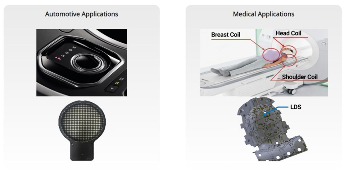
KYOCERA AVX’s LDS antennas establish seamless electrical connections in a wide variety of substrates, enhancing wireless performance and harmonising mechanical design attributes. Post-manufacturing surface finishes align the antennas with modern industrial design aesthetics and durability. A broad range of applications utilise KYOCERA AVX’s LDS antennas, including the Consumer Electronics (Mobile Phone, Notebook and Tablet Computers, Wearables etc), IoT Devices, Wireless Switches/Routers, Wireless Earphones/Earbuds, Healthcare / Medical Devices, Gaming Consoles, Automotive Navigation & Tracking Systems, Drone or Unmanned Aerial Vehicles (UAVs), High Security (Tamper Protection), Satellite Communications, Point of Sale (POS), Electronics Packaging and Connectors and Switches
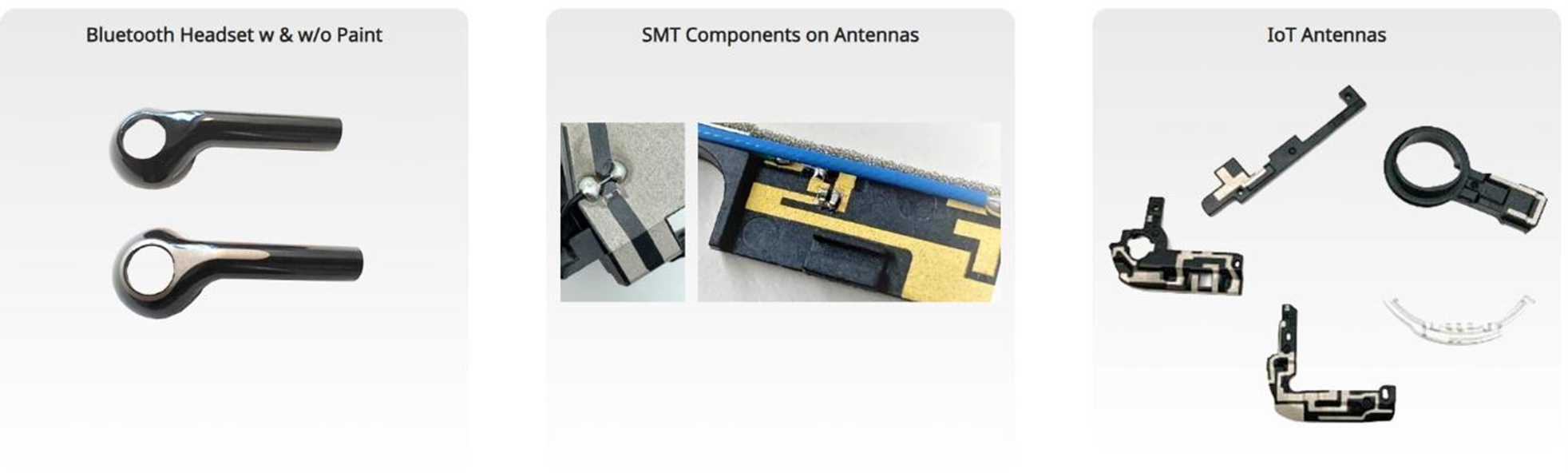
Non-Antenna LDS Applications
While antenna fabrication remains a prevalent application of LDS, the technology is instrumental in the development of various MIDs. LDS opens up a world of possibilities for product design, such as 3D PCBs, and minimises device weight by substituting traditional components like cables.
Conclusion
Laser Direct Structuring technology is a manufacturing process in which a conductive trace can be implemented directly on an injection moulded plastic. Its application extends to various fields, including manufacturing components such as antennas. The process, which involves injection moulding, laser structuring, and metallisation, establishes conductive structures within plastic substrates with the flexibility to integrate complex mechanical designs in miniature 3D shapes. The LDS technology advantages position it as a sustainable trend in a market driven by miniaturisation and efficiency demands. KYOCERA AVX’s LDS antennas enhance wireless performance in a wide range of substrates while harmonising with modern design for optimal durability and aesthetic appeal.
To read more content like this from KYOCERA AVX, please visit: https://www.kyocera-avx.com/category/technical-info-papers/