Europe's Cutting-Edge EV Lab: onsemi's Newest Innovation
In The News | 06-12-2023 | By Jack Pollard
onsemi, a trailblazer in the semiconductor sector, recently unveiled its latest endeavour: a state-of-the-art application test lab located in Piestany, Slovakia. This facility stands as a beacon of innovation, particularly in the development of electric vehicle (EV) and energy infrastructure (EI) technologies.
The lab is uniquely equipped for in-house testing, enabling the development of next-generation innovations. This capability is crucial for rapidly advancing automotive and power conversion technologies.
Enhancing xEVs and EI Systems: A Strategic Vision
The lab’s mission is twofold: to significantly advance the system solutions for xEVs and EI power conversion systems and to address the critical demands of the rapidly evolving semiconductor industry. By focusing on cutting-edge semiconductor technologies, the lab is poised to catalyse transformative improvements in system efficiency and performance. This pioneering initiative not only highlights onsemi’s dedication to technological excellence but also underscores its commitment to steering the electronic systems sector towards a more sustainable and energy-efficient future.
In its pursuit of advancing semiconductor solutions, the lab collaborates closely with automotive OEMs, Tier 1s, and EI providers. This collaborative approach ensures the development of solutions that are not only innovative but also aligned with industry needs and standards.
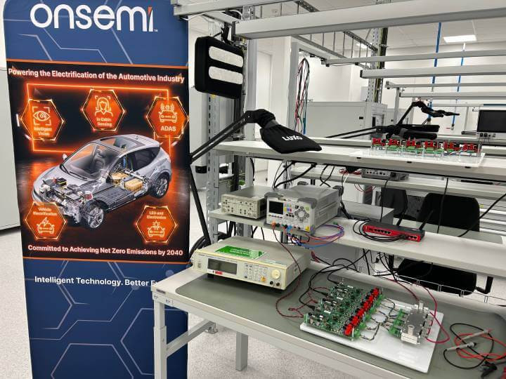
Exploring the Lab’s Advanced Capabilities and Impact
onsemi’s new lab in Piestany is a marvel of modern engineering, boasting advanced capabilities that set new standards in semiconductor development. The heart of its innovation lies in its high-voltage power labs, meticulously designed for both systems and device-level development.
These labs focus on pushing the boundaries of SiC/Si traction inverters and ACDC/DCDC power converters, fundamental components in modern power systems. Coupled with these are the lab’s cutting-edge facilities, including advanced equipment for laser welding, clean rooms, and workshops. These installations are not merely tools; they are catalysts of innovation, enabling onsemi to drive forward the efficiency, reliability, and overall performance of power systems, shaping the future of the semiconductor industry.
The lab houses two high-voltage power labs dedicated to systems and device-level development. It is equipped with laser welding facilities, mechanical clean rooms, and workshops, enhancing its capabilities in fast prototyping and testing of next-generation system solutions.
The lab’s evaluation capabilities are extensive, featuring continuous 24/7 testing, internally developed software and hardware for high-voltage power cycling, and high-accuracy devices for assessing SiC and Si health. Additionally, the lab can simulate extreme temperature conditions and program FPGAs and ARM microcontrollers, further supporting advanced research and development.
Driving Forward with Advanced Semiconductor Solutions and Sustainability
At the core of onsemi’s innovative leap is the development of advanced semiconductor solutions, specifically in the realms of silicon (Si) and silicon carbide (SiC) technologies. These developments are not just technical achievements but represent a paradigm shift in how power systems are conceptualised and realised.
Alongside these technological breakthroughs, onsemi demonstrates a profound commitment to environmental sustainability. The lab’s operations are designed with sustainable practices at their core, reflecting a deep understanding of the environmental considerations crucial in today’s world. This blend of high-end technological innovation with a strong environmental ethic positions onsemi as a leader in both advancing semiconductor technology and championing sustainable practices within the industry.
Concluding Insights and the Lab’s Industry Influence
The new onsemi lab in Piestany is poised to be a game-changer in the semiconductor industry, raising questions about its potential impact and innovative approaches.
FAQs: Unveiling onsemi’s Cutting-Edge Developments
- Q: How will the lab’s research advance power conversion systems in xEVs and EI?
- A: The lab is focusing on new topologies, modules, cooling systems, and advanced monitoring of power semiconductors. These developments aim to ensure high reliability and offer improved efficiency, reducing costs and enhancing gross margins ($/kW or GM).
- Q: How do the lab’s developments in Si and SiC semiconductor solutions impact electronic systems?
- A: Beyond advanced Si/SiC semiconductors, the lab is innovating in system packaging to minimise parasitic losses, thereby enhancing power density, system efficiency, and cost-effectiveness. These technologies are integral to the future of EV traction and EI applications, offering lightweight and high-performance solutions.
- Q: What are the lab’s approaches to sustainability in semiconductor development?
- A: Committed to sustainability, the lab adheres to net zero carbon footprint guidelines. It utilises the redundant heat from high-power semiconductor testing for heating its premises and employs high-power equipment with energy regenerative functionalities, saving up to 70% of otherwise wasted electric power.
These insights from onsemi not only reveal the lab’s strategic direction but also showcase its commitment to revolutionising electronic systems with a focus on efficiency, performance, and sustainability.