Four Things You Need to Know About Electron Microscopes
Articles | 13-05-2020 | By Gary Elinoff
The electron microscope allows magnifications of about ten million times, as compared to the one or two thousand times possible with a classical optical microscope. It empowers researchers to delve into realms not previously accessible to them.

An Electron Micrograph image of the Coronavirus
Credit. The Centers for Disease Control and Prevention
It is one of the main reasons that scientists are no longer “flying blind” when investigating viruses, and also empowers investigators in the field ranging from semiconductors to metallurgy and beyond.
1-The Nature of Vision
The reason you can see things is that light waves bounce off them. The colours that we perceive depend on the size of those wavelengths. At around 700 nanometers, we see red, and at about 400 nanometers, we see violet. That’s the extent of human vision; we can’t see wavelengths below 400 nanometers or above 700 nanometers.
The trouble comes in when we try to see things that are smaller than 400 nanometers, like details of a virus whose total length is only about 30 nanometers. To get any information, a structure that little has to be hit with a wavelength much smaller, which is where electrons come in.
Now, you’ve probably heard of the dual nature of light – sometimes it’s easier to describe it mathematically as a particle, and in other instances, a wave. Electrons, which we often think of as tiny particles, can also be thought of as waves. A beam of electrons can also be described as a wave whose wavelength is about one nanometer.
So, for garnering “visual” information about viruses, a beam of electrons fits the bill, and this is the basis of electron microscopy.
2- Scanning Electron Microscope
A scanning electron microscope (SEM) includes an electron source that forms a beam of electrons, which bombards an individual point on a sample to be studied with a beam of electrons. The electrons can be directed to a spot on the specimen as small as 1 nanometer.
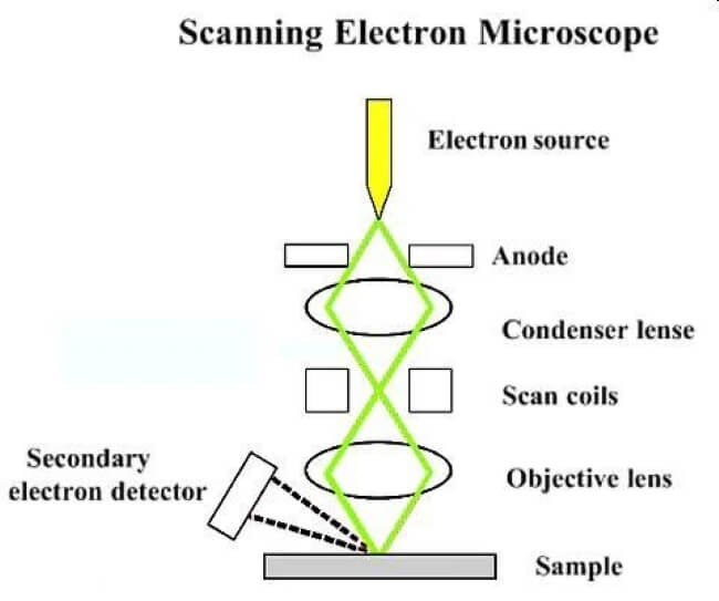
Basic components of a Scanning Electron Microscope
Credit: Thermofisher
A primary electron from the beam causes the specimen point to emit what are called secondary electrons. These secondary electrons, emitted from the sample, are recorded by a secondary electron detector. The number of reflected electrons are recorded in computer memory, with many electrons signifying a bright spot, and fewer electrons signify a dark spot.
Next, the electron beam is directed to a spot just to the right of the first. Here too, the number of reflected electrons are detected by the secondary electron detector and recorded in a computer. The process is continued, recording spots along the line, until the entire width of the specimen to be sampled is covered.
In the next step of the process, the electron gun is returned to a point slightly lower than the original position. It then begins to process the second row in the same manner as it did the first. The sequence is repeated until as many rows as desired are processed.

Raster scanning.
Modified Image Credit: Sherbrooke University
The process is called raster scanning. Computer memory holds information on every point on the multiple rows. For each point, many electrons recorded will signify a bright spot, while fewer electrons signify a dark spot.
The recorded dot is retrieved from the electron microscope’s computer memory can then be displayed, spot by spot, row by row on a display screen. The many thousands of spots scanned will display a black and white image of the sample studied.
3- Transmission Electron Microscope
Transmission electron microscopes (TEM) work by observing the electrons that are transmitted, or pass through, a sample to create an image. Thus, while SEMs render 2D mages of the surface of a sample, TEMs offer 3D details of the inner structure of the item under analysis.
TEMs also have far higher resolution, and can report details as small is 50 picometers. However, the samples analyzed by TEMs must be very thin, on the order of 100 or 200 nanometers,
![]()
Transmission Electron Microscope
Modified Image Credit: University of Warwick
The electron gun generates a beam of electrons, and it is tightly focused by the condenser system. The beam then strikes the specimen and depending on specimen thickness, and electron transparency, parts of it are transmitted.
A series of lenses focuses and channels the image. It is then focused on a fluorescent screen for viewing. The darker area of the projected image represent areas of the sample where electrons are impeded, while the lighter areas of the sample that allow more electrons to pass.
4- Electron Microscope Images and Color
The reader will note that both scanning and transmission electron microscopes produce only black and white images. As indicated by Smithsonian Magazine, “It could plausibly be said that colour doesn’t exist at that scale, because the things imaged by an electron microscope are smaller than the wavelength of visible light.” But yet, electron microscope images in both popular and professional publications almost always display blazing colours. Why? How?
In some cases, the colours are merely artists perceptions, based on guidance from the scientists who employ them.
There is also a methodology termed pseudocolour, or false colour, whereby a lookup table matches each pixel's intensity to a colour from the visible spectrum. In the image below, the left side illustrates a raw electron microscope image, and the right side shows a pseudocolour image.

Pseudocolour Electron Microscope Images
Modified Image Credit: Cambridge Core
Another method involves chemically “tagging” the proteins of sample metals. The electron microscope is enabled to separately distinguish the differently tagged proteins, and assign then different colours in the image.
With the advent of artificial intelligence, newer methodologies based on evermore subtle clues are now being developed.