Photonics Technology Will Bring Fast Internet to the Masses, Not Politicians
| 25-11-2019 | By Paul Whytock
As we move inexorably towards the new Christmas pantomime, or General Election as it's more usually called, the subject of high-speed Internet has become a political weapon.
This comes as no surprise given this country’s appalling lack of progress in implementing fast networks. To put that criticism in perspective the UK languishes in 34th place in the global league table of high-speed Internet with a national average broadband speed of 22.37MB/sec. This is below Madagascar and just about every European country and way below the Taiwanese national average of 85.02 MB/sec.
Politicians know the UK’s ponderous broadband is losing this country’s businesses money and making life difficult for many of their electorate who want to be a part of the fast Internet age.
Hence the trumpeting of political promises that always precede an election that everyone will have high-speed broadband if they elect a given political party.
Let's forget the politicians’ promises and their possibly inaccurate cost estimates on what budget would be required to make such promises a reality. Instead, let's look at a technology which can help to make ultra-fast light-based data transmission via the Internet a reality.
Photonics Technology Breakthrough
Breakthroughs in photonics technology really are helping with this and recent innovations will ensure extremely rapid and a more secure Internet in the future.
We are all familiar with the term quantum computing that suggests data processing will become three million times faster than the current fastest computers. So, what about quantum Internet?
One technology that could hold the key to making that a reality is silicon photonics. It was recognised some time ago that it could transmit data much faster than conventional technology.
However, although the technical theory was totally correct the age-old problem of meeting the production costs of turning theory into reality was a major hurdle. The problems lay in the area of how to integrate photonic capability into conventional integrated circuits.
But despite that, key technical breakthroughs are being made which is fortunate given the world's voracious appetite for information that consumes gargantuan quantities of data processing capability. Let's take a look at a few.
Three years ago industry experts estimated that the planet’s huge data centres were consuming almost 40% more electricity than the entire UK. Another challenge for our data-greedy world is that the volume of Internet use by ordinary citizens is creating data rates that are challenging the capability of conventional technologies. One example is that high-definition televisions are rendering conventional copper HDMI cables ineffective.
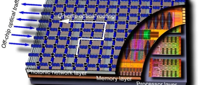
The solution is to create interconnects that employ photons rather than electrons. However, industry experts and photonic engineers and scientists know that manufacturing photonic-silicon devices isn’t easy.
There is one helpful aspect however and that is the photonics processes uses standard silicon wafers and much of the production equipment in today’s fabs to print optical components and circuitry onto wafers adjacent to other electronic elements.
But photons fundamentally do not behave in the same physical way that electrons do. Moving a photon from one element to another inside an IC is very tricky.
However, physicists at TUM have succeeded in accurately placing light sources in nano-thin material layers. This a key ground-breaking step that will make it possible to create quantum light sources in conventional three-dimensional materials such as diamond or silicon.
A layer of the semiconductor molybdenum disulfide was used as the material and this is only three atoms thick. They irradiated this with a helium ion beam which they focused on a surface area of less than one nanometre.
In order to generate optically active elements and the desired quantum light sources, molybdenum or sulphur atoms were very accurately processed out of the layer. The imperfections this created serve as traps for so-called excitons, electron-hole pairs, which then emit the desired photons.
In the future researchers also want to create more complex light source patterns in lateral two-dimensional lattice structures in order to examine multi-exciton phenomena or exotic material properties.
Another photonic technical breakthrough comes thanks to Finnish invention, the atomic layer deposition method.
Until now the rapid attenuation of light signals in microchips has prevented the use of light as a source of an information signal.
With international collaboration researchers at Aalto University have now developed a nano-sized amplifier to help light signals propagate through microchips.
The researchers have demonstrated that signal attenuation can be reduced when data is transferred inside a microchip, for example, from one processor to another.
The researchers also found that the atomic layer deposition method is very suitable for processing various kinds of microcircuits. To date the atomic layer deposition method has been used mainly in electronic applications. However, the indications are that applications could possibly exist in photonics.
The researcher also showed that a light signal can be potentially boosted in all kinds of structures and that the structure of a microchip is not limited to a specific type. The results indicate that atomic layer deposition is a promising method for developing microchip-photonic processes.
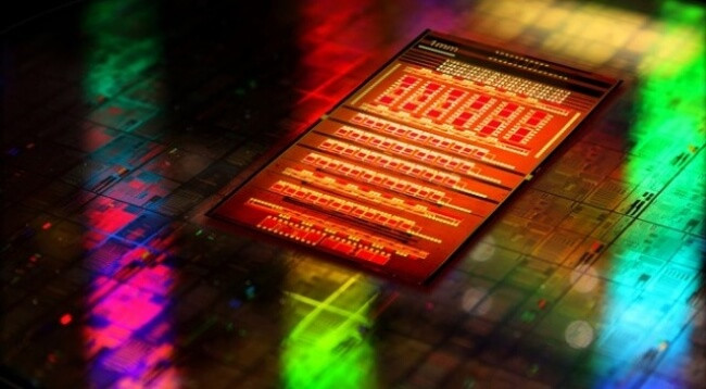
Credit: IBM Research | Silicon Integrated Nanophotonics
It’s clear that breakthroughs in materials for photonics applications will result in much faster Internet speeds but the eternal question is when?
The simple answer is not yet but we know it must inevitably happen. Some of the basic requirements are already happening. Photonic components must be very small scale, very power efficient and of course incredibly fast. However, meeting all those criteria simultaneously remains a challenge and as mentioned earlier being able to mass-produce accurately and at competitive costs is a long way off.
But thanks to the technological breakthroughs that art happening it is clear that when all the problems are solved there exists a huge €trillion annual market as photonics becomes the key in this planet’s global data-processing capabilities.
And there is, of course, one certainty regarding the availability of really high-speed Internet for the masses and that is whereas the promises made in political manifestos have a habit of fading over time the drive towards light-based technology will only accelerate.