From Pyrex to Processors: How Borosilicate Glass Is Transforming Mems Fabrication
Articles | 30-09-2015 | By Paul Whytock
The constant engineering drive towards ever flatter and thinner silicon wafers has received a significant boost following the development of new laser de-bonding techniques involving Borofloat, a borosilicate glass. Borofloat glass is widely used as a substrate material for MEMS (Micro-Electro-Mechanical Systems) processes due to its high flatness and thermal stability.
Its primary application in MEMS is as a carrier wafer for the temporary bonding of silicon wafers during the thinning process. Borofloat glass is also used in microfluidic devices and optical components due to its high chemical and thermal stability, making it suitable for harsh environments. It can be patterned and etched to create microchannels for fluid flow and used as a sacrificial layer in MEMS fabrication processes.
Introduction to Borofloat glass and its role in MEMS processes
There is nothing new about borosilicate glass. It was first developed by German glassmaker Otto Schott in the late 1800s and sold under the brand name Duran. Then in 1915, Corning Glass Works introduced Pyrex kitchenware, and the name became a synonym for borosilicate glass. These days Borofloat borosilicate glass from the Schott technology group is well recognised as a standard material for a MEMS processes such as anodic bonding, mainly because of its characteristics of very accurate flatness and predictable thermal performance.
Anodic bonding is widely used to combine silicon wafers with borosilicate glass to cap MEMS and other electronic and optical parts or to seal microfluidic devices. A perfect match between the two substrates is critical to ensure good bonding behaviour.
The breakthrough from Schott has created new forms of de-bonding. Laser de-bonding through a glass carrier wafer made of BOROFLOAT glass is possible because of deep UV light transmission at the relevant laser wavelength range. This operational factor facilitates the production of larger and thinner silicon wafers in what is a perdurable production process.
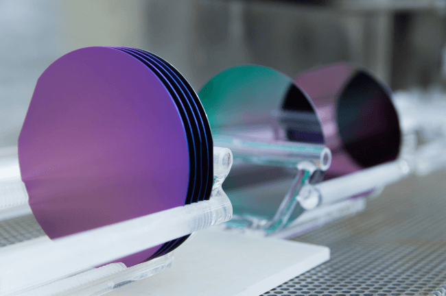
These are 100 mm silicon wafers grown in a cleanroom and placed in quartz holders after being in a silicon dioxide growth furnace. The wafers' colours depend on the thickness of the silicon dioxide layer and viewing angle, with common purples and greens adding a colourful touch to the cleanroom.
Laser de-bonding through Borofloat glass and its benefits
As mentioned previously, there is a constant drive towards smaller, lighter electronic devices with 3D design architecture, and this is attainable with ultra-thin silicon wafers with extreme flatness levels.
In addition to today's make-them-smaller-and-lighter design pressures, there is also the demand for higher yield rates, making larger and thinner wafers necessary.
The temporary bonding of a silicon wafer to a carrier wafer is a necessary step during silicon wafer thinning. The quality of a carrier wafer is determined by its ability to permit fast processing and de-bonding times and to achieve flawless surface cleanliness of the silicon wafer. Deep UV light transmission at correct laser wavelength ranges is imperative for this type of wafer de-bonding.
The Borofloat glass laser-activated release is achieved through irradiation using a high-power excimer laser at a low wavelength of 248 or 308 nm.
The thermal expansion characteristics of Borofloat glass over a wide temperature range are similar to silicon which is another important indication that makes it suitable for anodic bonding processes.
The suitability of Borofloat glass for anodic bonding processes
Borofloat glass is a favoured substrate material in MEMS processes because of its exceptional flatness and thermal stability. Its high abrasion resistance also makes it suitable for microstructure creation via several techniques, including ultrasonic drilling, powder blasting, photolithography and dry etching.
This particular feature endows Borofloat glass with remarkable mechanical strength and stability, making it an ideal substrate material for MEMS applications. Furthermore, the glass's chemical resistance allows it to withstand etching and chemical mechanical planarisation processes without any significant degradation or physical property changes. This feature guarantees that the glass maintains its structural integrity, ensuring high-quality and reliable MEMS devices.
All things considered, Borofloat glass's superior abrasion and chemical resistance make it an excellent choice for substrate material in MEMS fabrication processes. Its ability to withstand various microstructure creation and etching techniques ensures that the resulting MEMS device is of top-notch quality and reliability. As such, Borofloat glass is poised to continue playing a critical role in the advancement of MEMS devices in different industries.